- Submissions

Full Text
Research & Development in Material Science
Fabrication of Single Crystal Silicon Nanomembranes
Nicholas R Hemenway1 and Gokul Gopalakrishnan2*
1 Mechanical Engineering, University of Wisconsin, USA
2 Engineering Physics, University of Wisconsin, USA
*Corresponding author: Gokul Gopalakrishnan, Engineering Physics, University of Wisconsin, Platteville, USA
Submission: June 05, 2018; Published: June 26, 2018

ISSN: 2576-8840 Volume6 Issue5
Abstract
Silicon nanomembranes are thin, free standing sheets of single or poly-crystalline silicon, typically less than a micrometer thick, with lateral dimensions exceeding the thickness by several orders of magnitude. Nanomembranes have applications in flexible electronics, pressure sensing, photonic and phononic devices, sample mounts for microscopy, windows and beam splitters for optical and x-ray scattering measurements, and as a model system to perform fundamental investigations of nanoscale phenomena. This review covers fabrication processes for creating single crystal nanomembranes from a silicon-on-insulator (SOI) wafer as the starting material.
Introduction
Freestanding nanomembranes provide an ideal system for advancing nanoscience as well as for developing nanotechnologies. In addition to the advantages that crystalline silicon brings as an inexpensive semiconductor material with extremely well understood electronic and thermal properties and established processing methods, single crystal silicon membranes are particularly useful due to their superior mechanical properties: they are strong, flexible, stretchable, bondable and highly resistant to thermal and mechanical fatigue. The primary methods for fabricating single crystal nanomembranes use silicon-on-insulator (SOI) wafer as the base material, which also makes such devices easily compatible with SOI-based microelectronics.
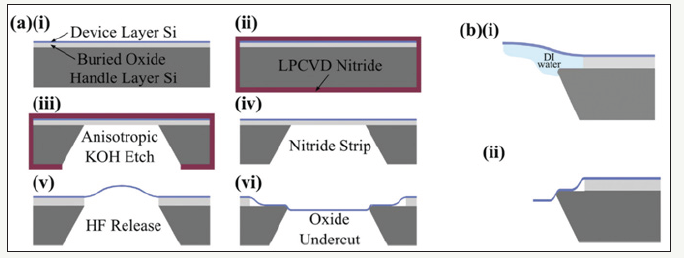
Figure 1:From [12] (a) Fabrication steps for producing nanomembranes from SOI. Parts (i) - (v) depict traditionally used silicon processing steps that typically result in buckled nanomembranes. Part (vi) is a modification to the process that flattens the membrane. (b) The mechanism for membrane flattening relies on the interfacial energy between silicon and water.

A primary hurdle in the fabrication of thin, flat nanomembranes arises from built-in compressive strains in the device layer of the SOI wafer. The fabrication process generally involves lithographic patterning and selective etching through the handle and buried oxide (BOX) layers of the SOI wafer, converting a selected region of the device layer into a freestanding membrane supported only along its edges (Figure 1). This process results in buckled nanomembranes due to the removal of the underlying support structure holding the compressively strained device layer in place [1-5]. The extent of buckling can be large enough to restrict the usefulness of the membrane structure, especially in microelectronic and micromechanical applications. Several approaches have therefore been used to mitigate this buckling and produce flat nanomembranes.
Discussion
One class of approaches is to completely release the membrane from the parent SOI and transfer it to a second frame. This can be done, for instance, by etching the BOX layer under the device layer through a series of etch holes and floating off the resulting membrane [6]. Another method involves a thermal expansion to compensate for the compressive device layer strains, followed by a direct wafer bonding step to transfer the device layer to a second substrate [7]. These techniques are particularly useful if a framing substrate other than the parent SOI wafer is desired.
On the other hand, several applications, especially those involving microelectronics and sensing have no need for a different framing substrate, or in fact, prefer the membrane to remain in its original SOI frame. A second class of approaches retains the membrane on the SOI wafer it was fabricated from, but uses one of several methods to flatten the membrane by compensating for the compressive strain in the device layer. For instance, significant flattening of the membranes can be achieved by patterning the device layer to create strain relief structures that accommodate the majority of the compressive strain, leaving the suspended membrane region relatively flat [1,8,9]. A more controlled approach that puts the membrane in tension uses a silicon nitride over layer to frame the edges of the membrane and introduce a tensile strain that overcomes the inherent compressive strain in the device layer [10,11].
An alternative approach to creating flat nanomembranes in the parent SOI embraces the phenomenon of stiction, which is painstakingly avoided in traditional MEMS fabrication. In this process, the interfacial energy between silicon and water is used to put the membrane in a meta-stable tensile state [12]. Buckling amplitudes on the order of several micrometers are replaced by flat membranes with thicknesses as low as 5nm and out of plane deviations no larger than 10nm over a region spanning more than 100μm across. These flat membranes can be subsequently stabilized by a directed UV exposure followed by a thermal anneal, which bonds the membrane more strongly to the underlying silicon ledges and relieves some of the tensile strain and strain in homogeneity in the membranes. Membrane tension is monitored through a series of pressure tests, whose results are compared with finite element models (FEM) of the membrane deflection under uniform pressure loading (Figure 2).
Figure 2:(a) Deflection of a 100nm thick membrane at a pressure of 20psi, measured by white light interferometry. (b) FEM solution of the same membrane under the same conditions. (c) Membrane strain map from the FEM analysis. Note: Displacements in the z-direction are exaggerated to display the membrane shape.

Conclusion
Several processes have been developed for the fabrication of thin, flexible single crystal silicon nanomembranes. These membranes serve as model systems to investigate nanoscale size effects on electronic transport [13,14], phonon dispersions [15-19] and heat transfer [20,21]. Further modification of the membranes by lithographic patterning [22] or strain engineering [23] leads to additional functionalities such as photonic devices and flexible electronics. Recent work has extended the use of these techniques to other materials, such as germanium, silicon-germanium multilayers, and silicon-silicon dioxide hetero-structures [24-26] further expanding the scope of potential applications.
References
- Iwase E, Hui PC, Woolf D, Rodriguez AW, Johnson SG, et al. (2012) Control of buckling in large micromembranes using engineered support structures. J MicroMech Microeng 22(6): 065028
- Juodkazis S, Nishi Y, Misawa H, Mizeikis V, Schecker O, et al. (2009) Optical transmission and laser structuring of silicon membranes. Optics Express 17(17): 15308-15317.
- Utteridge SJ, Sashin VA, Canney SA, Ford MJ, Fang Z, et al. (2000) Preparation of a 10nm thick single-crystal silicon membrane selfsupporting over a diameter of 1mm. Appl Surf Sci 162-163: 359-367.
- Striemer CC, Gaborski TR, McGrath JL, Fauchet PM (2007) Charge and size-based separation of macromolecules using ultrathin silicon membranes. Nature 445(7129): 749-753.
- Torres CMS, Zwick A, Poinsotte F, Groenen J, Prunnila M, et al. (2004) Observations of confined acoustic phonons in silicon membranes. Phys Status Solidi C 1(11): 2609-2612.
- Roberts MM, Klein LJ, Savage DE, Slinker KA, Friesen M, et al. (2006) Elastically relaxed free-standing strained-silicon nanomembranes. Nat Mater 5: 388-393.
- Delachat F, Constancias C, Fournel F, Morales C, Le Drogoff B, et al. (2015) Photosensitive polyamines for high-performance photocontrol of dna higher-order structure. ACS Nano 8(4): 3654-3663.
- Graff JW, Schubert EF (2000) Limitation of a localized surface plasmon resonance sensor for salmonella detection. Sens Actuator A-Phys 141(1): 276-283.
- McElhinny KM, Gopalakrishnan G, Savage DE, Silva-Martinez JC, Lagally MG, et al. (2015) Fabrication of flat SiGe heterostructure nanomembrane windows via strain-relief patterning. J Phys D: Appl Phys 48: 015306.
- Constancias C, Dalzotto B, Michallon P, Wallace J, Saib M (2010) Fabrication of large area ultrathin silicon membrane: Application for high efficiency extreme ultraviolet diffraction gratings. J Vac Sci Technol B 28(1): 194.
- Shchepetov A, Prunnila M, Alzina F, Schneider L, Cuffe J, et al. (2013) Ultra-thin free-standing single crystalline silicon membranes with strain control. Appl Phys Lett 102(19): 1-4.
- Gopalakrishnan G, Czaplewski DA, McElhinny KM, Holt MV, Silva- Martinez JC, et al. (2013) Fabrication of flat SiGe heterostructure nanomembrane windows via strain-relief patterning. Journal of Physics D: Applied Physics 48(1): 015306.
- Zhang PP, Nordberg EP, Park BN, Knezevic I, Evans PG, et al. (2006) Electrical conductivity in silicon nanomembranes. N Jour Phys 8: 200.
- Peng W, Aksamija Z, Scott SA, Endres JJ, Savage DE, et al. (2013) Probing the electronic structure at semiconductor surfaces using charge transport in nanomembranes. Nature Comm 4: 1339.
- Gopalakrishnan G, Holt MV, McElhinny KM, Spalenka JW, Czaplewski DA, et al. (2013) Thermal diffuse scattering as a pro. Phys Rev Lett 110: 205503.
- Gopalakrishnan G, Holt MV, McElhinny KM, Czaplewski DA, Evans PG (2013) probing large wave vector phonons at the nanoscale via x-ray thermal diffuse scattering. Adv X-ray Anal 56: 82.
- McElhinny KM, Gopalakrishnan G, Holt MV, Czaplewski DA, Evans PG (2017) Three-dimensional phonon population anisotropy in silicon nanomembranes. Phys Rev B 96(1): 014301.
- McElhinny KM, Gopalakrishnan G, Savage DE, Czaplewski DA, Lagally MG, et al. (2016) Synchrotron x-ray thermal diffuse scattering probes for phonons in Si/SiGe/Si trilayer nanomembranes. MRS Advances 1(48): 3263-3268.
- Cuffe J, Chavez E, Shchepetov A, Chapuis PO, El Boudouti EH, et al. (2012) Phonons in slow motion: dispersion relations in ultrathin Si membranes. Nano Lett 12(7): 3569-3579.
- Schroeder DP, Aksamija Z, Rath A, Voyles PM, Lagally MG, et al. (2015) Thermal resistance of transferred-silicon-nanomembrane interfaces. Phys Rev Lett 115(25): 256101.
- Neogi S, Reparaz JS, Pereira LFC, Graczykowski B, Wagner MR, et al. (2015) Tuning thermal transport in ultrathin silicon membranes by surface nanoscale engineering. ACS Nano 9(4): 3820-3828.
- Xu X, Subbaraman H, Chakravarty S, Hosseini A, Covey J, et al. (2014) Flexible single-crystal silicon nanomembrane photonic crystal cavity. ACS Nano 8(12): 12265-12271.
- Choi WM, Song J, Khang DY, Jiang H, Huang Y, et al. (2007) Biaxially stretchable “wavy” silicon nanomembranes. Nano Lett 7(6): 1655-1663.
- Rhead SD, Halpin JE, Shah VA, Myronov M, Patchett DH, et al. (2014) Tensile strain mapping in flat germanium membranes. Appl Phys Lett 104(17): 172107.
- McElhinny KM, Gopalakrishnan G, Savage DE, Martinez JCS, Lagally MG, et al. (2015) Fabrication of flat SiGe heterostructure nanomembrane windows via strain-relief patterning. Phys D: Appl Phys 48(1): 015306.
- Peng W, Roberts MM, Nordberg EP, Flack F, Colavita PE, et al. (2007) Appl Phys Lett 90: 1183107.
© 2018 Gokul Gopalakrishnan . This is an open access article distributed under the terms of the Creative Commons Attribution License , which permits unrestricted use, distribution, and build upon your work non-commercially.
 a Creative Commons Attribution 4.0 International License. Based on a work at www.crimsonpublishers.com.
Best viewed in


.jpg)


 Editorial Board Registrations
 Submit your Article
 Refer a Friend
 Advertise With Us
.jpg)


.jpg)


.bmp)
.jpg)
.png)
.jpg)


.jpg)


.png)

.png)


.png)


