- Submissions

Full Text
Peer Review Journal of Solar & Photoenergy Systems
Recent Progress in Ferromagnetism of Two- Dimensional Materials
Julienne Impundu1,2, Tariq Abbas3, Balla Diop Ngom4* and Sabir Hussain5*
1CAS Key Laboratory of Nano system and Hierarchical Fabrication, CAS Center for Excellence in Nanoscience, National Center for Nanoscience and Technology, China
2University of Chinese Academy of Sciences, China
3Department of Chemistry, Division of Science and Technology, University of Education, Pakistan
4Department of Solid-State Physics and Engineering Science, University Cheikh Anta Diop of Dakar, Senegal
5Tyndall National Institute, University College Cork, ‘Lee Maltings’, Dyke Parade, Cork T12 R5CP, Ireland
*Corresponding author: Balla Diop Ngom, Laboratory of Quantum Photonics, Energy and Nanofabrication, Department of Solid State Physics and Engineering Science, University Cheikh Anta Diop of Dakar, Senegal Sabir Hussain, Tyndall National Institute, University College Cork, ‘Lee Maltings’, Dyke Parade, Cork T12 R5CP, Ireland
Submission: June 27, 2023;Published: September 21, 2023

Volume2 Issue4 September , 2023
Abstract
Two-dimensional (2D) materials are appealing for nanoelectronics due to their distinct physical characteristics and ultimate thickness dimension. Using these nanomaterials will be advantageous for many developing spintronic device designs and provide a more incredible method for controlling spin. Spintronics holds promise for the future of information technology, potentially replacing silicon-based complementary metal-oxide semiconductors that rely on charge manipulation. Still under investigation is the quest for discovering 2D materials with ferromagnetic properties, capable of generating, detecting, and controlling spin behavior. So, we are writing this mini-review to provide a concise summary of the recent advancements made in the field of ferromagnetism. Here we will summarize to encompass various aspects, such as the development of ferromagnetic 2D materials, their ability to produce, detect, manipulate spin behavior, and the implications of these findings in broader scientific and technological contexts.
Keywords:Ferromagnetic properties; Spintronics; Heterostructure; 2D Nanomaterials
Introduction
Ferromagnetism in 2D materials originates from the alignment of electron spins, resulting in a collective magnetic order where neighboring spins are parallel. This alignment can be achieved through various mechanisms, such as the presence of localized magnetic moments or the exchange interaction between itinerant electrons. The reduced dimensionality and unique properties of 2D materials play a crucial role in stabilizing ferromagnetic order at relatively high temperatures, which is not typically observed in bulk materials. Ferromagnetic 2D materials hold significant importance due to their potential applications in spintronic devices, magnetic sensors, and data storage [1,2].
Graphene, the first discovery of 2D material, developed in 2004 when Novoselov and Geim [3] succeeded in isolating a single layer of carbon atoms arranged in a honeycomb lattice with unique and fascinating physical properties. It opened up a new era in materials science and led to extensive research into 2D materials. It serves as a building block for constructing more complex 2D materials and has found applications in fields ranging from electronics and photonics to energy storage and biomedical devices [3].
Ferromagnetism has also been observed in several 2D materials beyond graphene. For instance, well know monolayer MoS2, MoSe2, WS2 and so on have exhibited ferromagnetic behavior when subjected to certain conditions, such as strain, defects, or doping. Additionally, Van Der Waals (vdW) magnets like CrI3 and Fe3GeTe2 have shown robust ferromagnetic properties in their 2D form. Moreover, combining different 2D materials in vdW heterostructures allows for the engineering of tailored magnetic properties and interlayer exchange interactions. The exploration of ferromagnetism in these diverse 2D materials and vdW heterostructures presents exciting prospects for advancing spintronics, magnetic storage, and other technological applications [4-6].
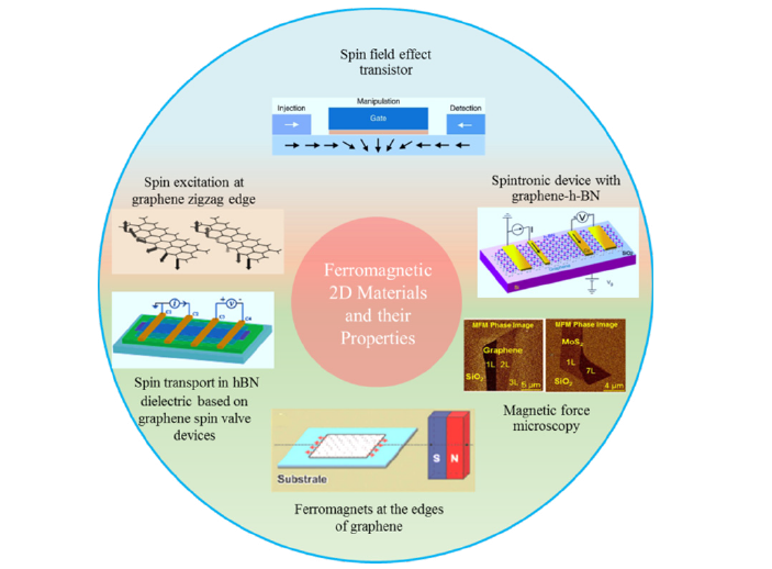
In this mini-review, research into the ferromagnetism in 2D materials has taken many directions, particularly in the field of spintronics, as shown in Figure 1. This evolution is due to a variety of techniques, some of which are purely technical, such as the increased use of Magnetic Force Microscopy (MFM), which is used to analyze the local magnetic behavior of nanomaterials [7]. This system functions in non-contact mode using a ferromagnetic tip as a local field sensor. As a result, images of the spatial variation of magnetic forces can be viewed on a sample surface, showing both its topography and magnetic properties. Moreover, the MFM provides the highest resolution and details regarding the magnetization process in general [8] and the magnetization reversal [9,10] of magnetic materials. Spintronics devices utilize the intrinsic spin property of electrons to manipulate and store information, enabling faster and more energy-efficient electronic devices. They hold promise for next-generation technologies such as magnetic memory, spin-based logic devices, and quantum computing. Additionally, a lot of research has gone into understanding the magnetization response that spintronics devices exhibit [10-14].
Figure 1:Structural properties, characterizations and device applications based on ferromagnetic 2D materials [2,10-14].

Central Concept of Ferromagnetic 2D Materials and Application
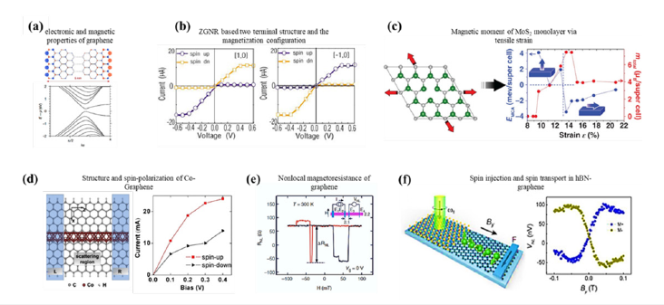
The paramagnetic behavior has been observed in 2D materials due to the presence of unpaired electrons and high density of states near the Fermi level. Where the favorable electronic structures and strong exchange interactions align the neighboring magnetic moments, resulting in a net magnetic moment. Kim et al. [15], Kou et al. [16], Yazyev and Helm [17] have predicted that magnetism (Figure 2) will result from both the edge states that develop around zigzag-shaped edges [15,16] and defects that either vacancy or hydrogen chemisorption [17,18]. Cervenka et al. [19], Zhou et al. [20] have revealed the presence of ferromagnetic localized on order at the edges of graphite and n-layer graphene [19,20]. In addition, the available literature from Zhou et al. [20] has shown that local magnetic moments exist at the edges of n-layer graphene and graphite with a Curie temperature above ambient temperature [11]. On the other hand, Yazyev et al. [21] have exposed that both transverse and longitudinal fluctuations of magnetic moments at the zigzag edges of graphene from the first principles have been studied as well. It has been found that due to the transverse fluctuations resulting from a high spin stiffness constant, the spin correlation length at ambient temperature is 1nm. Under the critical temperature, the spin correlation length increases significantly, while at temperatures exceeding 10K, the spin correlation length decreases due to weak magnetic anisotropy [21].
Figure 2:Structures and Graphs explain ferromagnetism of 2D nanomaterials. (a) Magda et al. [22] show the correlation between the electronic and magnetic properties of ZGNs. (b) Zeng [23] and colleagues determined the spin-dependent electron transport properties of 8-ZGNR. (c) Yun et al. [24] propose a diagrammatic representation of the magnetic moment of the MoS2 monolayer induced by tensile strain. (d) Jiang et al. [25] establish the design of the two-probe model apparatus and its Spin-dependent I-V curves. (e) Measurement of nonlocal magnetoresistance on a graphene nonlocal spin valve with tunneling contacts done by Han [26] and his colleagues. (f) Sierra et al. [27] obtained optical spin injection and spin transport.

Further improvements in ferromagnetism behavior were observed when different research groups have conducted density functional theory calculations to investigate the strain-induced electronic and magnetic properties of single-layer MoS2 with vacancy defects [22-27]. It has been observed that the application of tensile strain induces ferromagnetic behavior and transforms the material into a metallic state [24]. They then used cobalt electrodes to demonstrate spin injection into graphene at ambient temperature. Where it is also possible to detect spin by contrasting the spin-up and spin-down local currents. Nevertheless, both weak spin-orbit coupling, and its zero bandgap prevent it from being used to create sophisticated spintronic devices like logic gates [28]. Now that straightforward experimental methods have been developed for coupling graphene with other atomically thin vdW crystals to generate heterostructures has made it possible to examine the characteristics of vdW heterostructures [29].
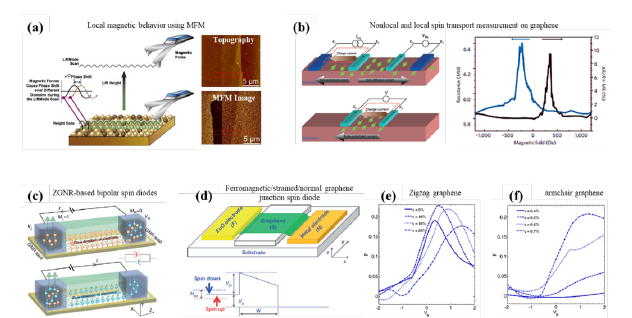
Figure 3:MFM and magnetic devices. (a) The topography and phase images of graphene nanosheets captured by AFM and MFM, respectively, are represented by Wang [10] and his colleagues. (b) Configurations for nonlocal and local spin transport measurement done by Han et al. [26] (c) Zeng et al. [23] proposed a schematic representation of bipolar spin diodes based on ZGNR. (d) Wang et al. [30] spin diode diagram. The spin diode comprises a junction of graphene that is ferromagnetic, strained, and normal. (e and f) Graph showing the relationship between spin polarization and the bias voltage Vb. The effects of the strain caused by the zigzag direction and the effects of the strain caused by the armchair’s direction are represented respectively..

However, there are still numerous unanswered questions, and some of them are addressed in this mini-review. It is undoubtable that readers will come up with more to be added to the list. However, A new class of magnetic devices for magnetic storage, sensing, and data processing would be possible if 2D nanostructures could be used to effectively and reliably produce nanosized carbon materials that are magnetic. Eventually, these concerns are to enhance the innovative nature of the experimental study in this field and its promising future [30] (Figure 3).
Summary and Challenges
Recent progress in the field of ferromagnetism in 2D materials has shown great promise for various applications namely spintronics, magnetic memory devices, magnetic sensors, spin filters, magnetic heterostructures, and magnetic probes. Here we have described some techniques like doping, defect engineering, and proximity effects have been employed to induce and manipulate ferromagnetism in these materials. However, challenges still remain, including understanding spin relaxation in materials like graphene, studying magnetic interactions in graphene, addressing environmental effects and material degradation in TMDCs, overcoming limitations in achieving room temperature spintronic applications involving magnetic vdW materials, and developing diluted magnetic systems for TMDCs. Overcoming these challenges will be crucial to fully harness the potential of 2D ferromagnetic materials and realize their practical applications in various fields.
Acknowledgement
The first author acknowledges the financial support from Organization for Women in Science for the Developing World (OWSD) Postgraduate fellowship program and Swedish International Development Cooperation Agency (SIDA).
References
- Zhang G, Guo F, Wu H, Wen X, Yang L, et al. (2022) Above-room-temperature strong intrinsic ferromagnetism in 2D van der Waals Fe3GaTe2 with large perpendicular magnetic anisotropy. Nat Commun 13: 5067.
- Feng YP, Shen L, Yang M, Wang A, Zeng M, et al. (2017) Prospects of spintronics based on 2D materials. Wires Comput Mol Sci 7(5): e1313.
- Novoselov KS, Geim AK, Morozov SV, Jiang D, Zhang Y, et al. (2004) Electric field effect in atomically thin carbon films. Science 306(5696): 666-669.
- Mak KF, McGill KL, Park J, McEuen PL (2014) The valley hall effect in MoS2 Science 344(6191): 1489-1492.
- Wang Z, Gutiérrez-Lezama I, Ubrig N, Kroner M, et al. (2018) Very large tunneling magnetoresistance in layered magnetic semiconductor CrI3. Nat Commun 9: 2516.
- Huang B, Clark G, Navarro-Moratalla E, Klein DR, Cheng R, et al. (2017) Layer-dependent ferromagnetism in a van der Waals crystal down to the monolayer limit. Nature 546(7657): 270–273.
- Li H, Qi X, Wu J, Zeng Z, Wei J, et al. (2013) Investigation of MoS2 and graphene nanosheets by magnetic force microscopy. ACS Nano 7(3): 2842-2849.
- Asenjo A García D, García JM, Prados C, Vázquez M (2000) Magnetic force microscopy study of dense stripe domains in Fe-B/Co-Si-B multilayers and the evolution under an external applied field. Phys Rev B 62(10): 6538-6544.
- Sorop TG, Untiedt C, Luis F, Kröll M, Raşa M, de Jongh LJ (2003) Magnetization reversal of ferromagnetic nanowires studied by magnetic force microscopy. Phys Rev B 67(1): 014402.
- Wang T, Wang Y, Fu Y, Hasegawa T, Li FS, et al. (2009) A magnetic force microscopy study of the magnetic reversal of a single Fe nanowire. Nanotechnol 20(10): 105707.
- Zhou H, Yang H, Qiu C, Liu Z, Yu F, et al. (2011) Experimental evidence of local magnetic moments at edges of n-Layer graphenes and graphite. J Phys Chem C 115(32): 15785-15792.
- Yazyev OV (2010) Emergence of magnetism in graphene materials and nanostructures. Rep Prog Phys 73(5): 056501.
- Gurram M, Omar S, Wees B (2017) Electrical spin injection, transport and detection in graphene-hexagonal boron nitride van der Waals heterostructures: Progress and perspectives. 2D Mater 5(3): 032004.
- Kamalakar MV, Dankert A, Bergsten J, Ive T, Dashb SP (2014) Spintronics with graphene-hexagonal boron nitride van der Waals heterostructures. Appl Phys Lett 105(21): 212405.
- Kim YH, Choi J, Chang KJ, Tománek D (2003) Defective fullerenes and nanotubes as molecular magnets: An ab initio study. Phys Rev B 68(12): 125420.
- Kou L, Tang C, Guo W, Chen C (2011) Tunable magnetism in strained graphene with topological line defect. ACS Nano 5(2): 1012-1017.
- Yazyev OV, Helm L (2007) Defect-induced magnetism in graphene. Phys Rev B 75(12): 125408.
- Yazyev OV (2008) Magnetism in disordered graphene and irradiated graphite. Phys Rev Lett 101(3): 037203.
- Cervenka J, Katsnelson MI, Flipse CFJ (2009) Room-temperature ferromagnetism in graphite driven by two-dimensional networks of point defects. Nat Phys 5(11): 840-844.
- Zhou H, Huaichao Y, Caiyu Q, Zheng L, Fang Y, et al. (2011) Aggregation of ferromagnetic and paramagnetic atoms at edges of graphenes and graphite. J Phys Chem B 20(2): 26803-026803.
- Yazyev OV, Katsnelson MI (2008) Magnetic correlations at graphene edges: Basis for novel spintronics devices. Phys Rev Lett 100(4): 047209.
- Magda GZ, Jin X, Hagymási I, Vancsó P, Osváth Z, et al. (2014) Room-temperature magnetic order on zigzag edges of narrow graphene nanoribbons. Nature 514(7524): 608-611.
- Zeng M, Shen L, Su H, Zhang C, Feng Y (2011) Graphene-based spin logic gates. Appl Phys Lett 98(9): 092110.
- Yun WS, Lee JD (2015) Strain-induced magnetism in single-layer MoS2: Origin and manipulation. J Phys Chem C 119(5): 2822-2827.
- Jiang CH, Chen Q, Ge GX, Li YB, Wan JG (2016) Structure and spin-polarized transport of co atomic chains on graphene with topological line defects. J Clust Sci 27: 875–882
- Han W, Kawakami RK, Gmitra M, Fabian J (2014) Graphene spintronics. Nat Nanotechnol 9: 794.
- Sierra JF, Fabian J, Kawakami RK, Roche S, Valenzuela SO (2021) Van der Waals heterostructures for spintronics and opto-spintronics. Nat Nanotechnol 16(8): 856-868.
- Ahn EC (2020) 2D materials for spintronic devices. NPJ 2D Mater Appl 4(1): 17.
- Yankowitz M, Ma Q, Jarillo-Herrero P, LeRoy JB (2019) Van der Waals heterostructures combining graphene and hexagonal boron nitride. Nat Rev Phys 1(2): 112-125.
- Wang Y, Liu Y, Wang B (2014) Graphene spin diode: Strain-modulated spin rectification. Appl Phys Lett 105(5): 052409.
© 2023 Julienne Impundu and Balla Diop Ngom. This is an open access article distributed under the terms of the Creative Commons Attribution License , which permits unrestricted use, distribution, and build upon your work non-commercially.
 a Creative Commons Attribution 4.0 International License. Based on a work at www.crimsonpublishers.com.
Best viewed in


.jpg)


 Editorial Board Registrations
 Submit your Article
 Refer a Friend
 Advertise With Us
.jpg)


.jpg)


.bmp)
.jpg)
.png)
.jpg)


.jpg)


.png)

.png)


.png)


