
- About Us
- Information
-

The Author ensures that the research has been conducted responsibly and ethically with adherence to all relevant regulations. read more..
- For Authors
- For Reviewer
- Manuscript Guidelines
- Membership
- Publication Ethics
-
- Journals
- Reprints
- e-Books
- Videos
- Policies
- Contact Us
 COVID-19
- Submissions


Full Text
Research in Medical & Engineering Sciences
Fabrication Process Development of Uniform Nanopatterns on Lens Surface Via the Control of Focus Distance in Laser Interference Lithography
Soonkyu Je*, Sangwon Hyun, Joongyu Park and Geonhee Kim
Department of Optical Instrumentation Development, Korea
*Corresponding author: Soonkyu Je, Department of Optical Instrumentation Development, Korea
Submission: December 10, 2019 Published: December 16, 2019

ISSN: 2576-8816Volume8 Issue3
Abstract
In recent years, the demand for optics has been increasing as research is conducted in optically diverse fields. Typical optics have flat shaped optics, such as mirrors, but some have curvature, such as lens. Flat optics make it easy to uniformly manufacture coatings or nanopatterns on surfaces, but it is difficult to uniformly manufacture coatings or nanopatterns on lens with curvature. Therefore, in this study, the curvature of the lens was measured and the spherical wave was created to match the curvature of the lens to produce a uniform pattern on the lens surface with curvature, creating a periodic nanopattern through laser interference lithography on the top of the lens. To check the uniformity of nanopatterns on the lens, several points were selected from the specimen to measure, compare and analyze the AFM and SEM image.
Nomenclature
λ = wavelength of laser
θ = incidence angle
n = refractive index
R = focal length of lens
R’ = focal length of spatial filter
Keywords: Laser interference lithography; Lens surface; Nanopatterns
Introduction
Recently, as various fields using optics have been actively developed, the demand for optical instruments has been increasing. Among them, more developed optics mounted on satellites due to the increasing number of various kind satellites. Optical systems used in satellites are large and reflective type because of their material properties. There is a lot of research going on to increase the light efficiency of these optics, among which there is a lot of research on the manufacture of surface coatings and patterns for increase the various optical efficiency. However, these optics are very large, have to use very expensive equipment for coating, and because of the multi-layer coating's characteristics, they are difficult to demonstrate efficiency with a single layer, resulting in a more expensive or difficult process [1,2].
In this study, as a basic technology for producing large-area nanopatterns on a surface of a curvature optics, PR coating was processed using spin coater on the surface of the lens, and the technology of fabricating nanopatterns uniformly on the surface of the lens, through the adjustment of the lens focal length of laser interference lithography to fabricate the anti-reflective pattern was proposed and fabricated [3-5]. This pattern was measured by AFM and SEM, and patterns were compared, and the validity of the technology was verified. Based on this technology, if beam size is expanded and applied to large-area optical systems, nanopatterns can be fabricated on various satellite optical systems.
Laser interference lithography system setup
Laser interference lithography is a technology that fabrication nano/micro patterns by exposure of interference two beams on photoresist. The two beams were used of the same single wavelength and the size of the interference pattern is shown as Equation 1.
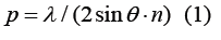
In equation 1, p is the period of fringe that results from interference of two beams, and λ is the wavelength of the laser, θ is the incidence angle, and n is the refractive index. Therefore, if θ reaches 90 degrees, up to half of the laser wavelength can be fabricated, and if n is higher, more small patterns can be made, but this is used only in special cases, and if normal laser interference lithography processes in the atmosphere, so n is 1 and θ is used between 0 and 90 degrees [6].
In order to show anti-reflective effects in the visible wavelength area, it needs a 2D pattern in the form of sinusoidal with an aspect ratio of 1 with a pattern pitch of 200 to 350nm. Therefore, we selected the pitch of pattern to be 300nm, the laser used 405nm wavelength to fabricate pattern of this pitch size, and incident angle of two beams are selected at 42.5 degrees. The beam was expanded using a spatial filter with the same R value according to the curvature of the lens, and the pattern in 2D format was fabricated by rotating it after exposure once and exposure again. In addition, to compare the two-beam laser interference lithography and Lloyd mirror laser interference lithography, each system was set up and experimented.
Two beam laser interference lithography
As shown in Figure 1, the two-beam laser interference system separated the beam from the laser into the beam splitter. Then, each beam was constructed in the R' position and the spatial filter was constructed to match the R value of the lens as shown in Figure 2. And the same spherical wave expanded beam was created by each spatial filter to an angle of incidence of 42.5 degrees. Then, the lens was set up at the point of the two beams interfered and we fabricated nanopatterns.
Figure 1: Two beam laser interference lithography system setup.

Lloyd mirror laser interference lithography
Lloyd mirror laser interference lithography system is a technology that can fabricate a laser interference pattern with simple system set up. In general, Lloyd mirror laser interference lithography can make a nanopatterns by optical system and a target holder with a large mirror and a specimen built at 90 degrees, the technology is to expand the beam to produce a large area laser interference pattern at once. Therefore, we expanded the beam through the spatial filter as shown in Figure 3 and set up the system by making jigs so that the mirror and the specimen holder are 90 degrees. The position of the spatial filter was placed in the position R' according to the R value of the lens as shown in Figure 4. Finally, we experimented of laser interference lithography for making a uniform nanopatterns on the lens surface.
Figure 2: Spatial filter setup by lens focal length in two beam laser interference lithography.

Figure 3: Lloyd laser interference lithography system.

Figure 4: Spatial filter setup by lens focal length in Lloyd mirror laser interference lithography.

Experimental Result
In order to fabricate nanopatterns on the surface of the lens, a photoresist (DPR-i7000) was applied uniformly through spin coater and soft baking (90°, 80 seconds) was performed. After the first exposure, for fabricating the 2D pattern we rotate the lens and experiment 2nd exposure. The first and second exposure were equally experimented for 90 seconds, and after the second exposure, the developing process was operated for 60 seconds. After exposure, lens was placed in DI water to clean and the water completely dried with an air gun. And then, we experimented hard baking process (120°, 120 seconds). The comparative analysis of the fabricated nanopatterns in this process confirmed that the results of the two-beam laser interference lithography experiment and the results of the lloyd mirror laser interference lithography experiment were not different.
In order to obtain optimum exposure and development time in the lloyd laser interference lithography process was checked by time, and patterns were most clearly visible in the 120 second exposure and 60 seconds developing. Nanopatterns made by rotating 60 degrees in secondary exposure were measured by AFM as shown in Figure 5, and patterns made by rotating 90 degrees were measured by SEM as shown in Figure 6. Measured in various areas of the lens, the error in the pitch or height of the pattern was within 1%.
Figure 5: AFM image of laser interference lithography nano patterns.

Figure 6: SEM image of laser interference lithography nano pattern.

Conclusion
In order to fabricate uniform nanopatterns on the surface of the lens, we set up a system that applies to laser interference lithography with a spherical wave and made uniform nanopatterns on the surface of the lens through experiments. Then, the nanopatterns were measured through AFM and SEM and the uniformity of the pattern was checked. Based on this process, laser beams were expanded to confirm that they could be applied to large area optics. When a finish the large satellite optical mirror or lens with 600mm, 800mm and 1000mm we have been developed, we will fabrication nanopatterns on the surface of the large area optical components.
Acknowledgement
We would like to acknowledge the financial support from the KBSI grant (T39120) and the National Research Council of Science & Technology of Republic of Korea (PN2019013).
References
- Xie Q, Hong M, Tan H, Chen G, Shi L, et al. (2008) Fabrication of nanostructures with laser interference lithography. Journal of Alloys and Compounds 449(1-3): 261-264.
- Zheng M, Yu M, Liu Y, Skomski R, Liou SH, et al. (2001) Magnetic nanodot arrays produced by direct laser interference lithography. Applied Physics Letters 79(16): 2606-2608.
- Spallas JP, Hawryluk AM, Kania DR (1995) Field emitter array mask patterning using laser interference lithography. Journal of Vacuum Science & Technology B: Microelectronics and Nanometer Structures Processing, Measurement, and Phenomena 13(5): 1973.
- Ainara R, Mikel E, Miguel E, Noemi P, Yuri V, et al. (2009) Laser interference lithography for nanoscale structuring of materials: from laboratory to industry. Microelectronic Engineering 86(4-6): 937-940.
- Murillo R, Wolferen H, Abelmann L, Lodder J (2005) Fabrication of patterned magnetic nanodots by laser interference lithography. Microelectronic Engineering 78(79): 260-265.
- Soonkyu J, Jongmyeong S, Joongeok K, Minsoo K, Jinhyung L, et al. (2013) Development of direct deep reactive ion etching process using laser interference lithographed etch barrier without intermediate layer. Japanese Journal of Applied Physics 52(10S): 10MC04.
© 2019 Soonkyu Je. This is an open access article distributed under the terms of the Creative Commons Attribution License , which permits unrestricted use, distribution, and build upon your work non-commercially.
Editor In Chief


.jpg)


Signup for Newsletter

Quick Links
 Editorial Board Registrations
 Submit your Article
 Refer a Friend
 Advertise With Us
Our Recent Edition

.jpg)


Top Editors


.jpg)


.bmp)
.jpg)
.png)
.jpg)


.jpg)


.png)

.png)


.png)


Financial Support

Sponsors

Latest e-Books

Latest Video

 a Creative Commons Attribution 4.0 International License. Based on a work at www.crimsonpublishers.com.
Best viewed in
a Creative Commons Attribution 4.0 International License. Based on a work at www.crimsonpublishers.com.
Best viewed in