- Submissions

Full Text
Research & Development in Material Science
Advancements in 2D Materials Based Thermoelectric Devices
Neeraj Dhariwal1*, Preety Yadav1, Manju Kumari1, Meenu Chahar2, Vinod Kumar1* and Thakur OP1
1Materials Analysis & Research Lab, Department of Physics, NSUT, India
2Department of Physics, Chaudhary Ranbir Singh University, India
*Corresponding author:Neeraj Dhariwal, Materials Analysis & Research Lab, Department of Physics, NSUT, Dwarka Sec-3, New-Delhi-78, India
Submission: May 05, 2025;Published: May 22, 2025
ISSN: 2576-8840 Volume 21 Issue 5
Abstract
In the present scenario, Two-dimensional (2D) materials have emerged as one of the promising candidates for harvesting some fraction of heat available in abundant around us via Thermoelectric (TE) device. Among many of the available 2D materials MXene, graphene, Black Phosphorous (BP) and two-dimensional (2D) metal dichalcogenides (TMDCs) have attracted lot of attention as high-performance materials due to their unique thermal, mechanical and optoelectronic properties owing to their enhanced see beck coefficient. Over the last few years, most of the research has been focused on enhancing the thermoelectric figure of merit (ZT) by material engineering, defect engineering, doping and hetero structure formation. Recent development in film formation, material synthesis and their optimization have provided better device quality, uniform layering and enhanced device performance. Additionally, inclusion of these materials in wearable and flexible electronics has opened new avenues for various applications. The present review provides a detailed discussion of recent development in 2D based thermoelectric devices including device formation, material innovation and fundamentals. Some of the key challenges such as scalability and environment stability has been also discussed. Lastly, we highlighted emerging 2D materials, future direction and innovations towards sustainable, cost effective and multifunctional energy generation solutions.
Keywords:Two-dimensional (2D) materials; Figure of merit (ZT); Seebeck coefficient; Thermoelectric
Introduction
Due to their remarkable ability to convert waste heat into useful electrical power, thermoelectric materials have gained attention as viable solutions to these issues. Enhancing performance, scalability, and applicability has become increasingly important in the study of thermoelectric materials and systems [1]. The dimensionless figure of merit (ZT), ZT=σS2T/κ, is used to assess the thermoelectric performance of the materials at a given temperature. The electrical conductivity, See beck coefficient, and absolute temperature are represented by the variables σ, T, and κ in this expression, respectively. Additionally, κL denotes the lattice thermal conductivity, κ(L) denotes the electronic thermal conductivity, and κ(e) denotes the electronic thermal conductivity [2,3]. These variables are closely related to one another and rely on the band and crystal structure of the material. It is nearly impossible to tune these three factors separately because of their intricate interrelation. However, in recent years, a number of records for the greatest ZT values have been consistently beaten as a result of the creation of new materials, processing methods, and concepts/mechanisms [4].
The last several decades have seen an incredible increase in scientific interest in these materials since the initial discovery of graphene in 2004 [5]. As new techniques for theoretical simulation and materials synthesis have emergedtechniques, numerous 2D materials have been successfully produced and predicted theoretically. Black phosphorus (BP), graphene, transition metal dichalcogenides (TMDCs) (such as MoS2, WS2, MoSe2, andMoTe2), Group IVA-VA compounds (such as SnSe, GeSe, and SnS), nitrides (such as boron nitride), MXenes (such as Ti3C2), andTi4N3), as well as MXenes (such as antimonene, arsenene, bismuthine, and black phosphorene) [6-8]. Various allotropes of these two-dimensional materials have exceptional optical and electrical characteristics. The 2D materials are solidifying their position and assuming a central role in this scene due to their atomic thinness. 2D materials are known as crystals and are often composed of single- or fewlayer atoms. They have strong covalent bonds within the plane and much weaker vander Waals (vdW) interactions outside of it. From a materials engineering standpoint, 2D materials are also defined as having lateral dimensions on the order of micrometers, which are larger than the transverse dimensions, which typically range around nanometers. This has led to their widespread use in bioapplication energy storage (such as batteries and supercapacitors), electronics, optoelectronics, topological spintronics, and energy conversion.
At present, a thorough study of 2D thermoelectric materials is lacking, despite the fact that intriguing research findings in both theoretical predictions and testing have been attained. It is essential to concentrate on the advancements in this field of study in order to foster their growth. In addition to exploring the potential effects and future prospects of these developments, this study attempts to present a thorough review of the most recent developments in 2D based thermoelectric materials and fillers along with their wide range of applications in many industries.
The potentials 2D thermoelectric materials
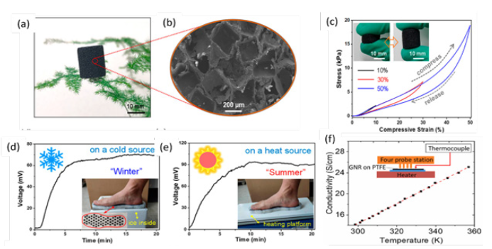
Graphene: The inherent advantages of graphene, such as its nontoxic composition, lightweight nature, high mechanical flexibility and thermal stability, ultrahigh intrinsic carrier mobility (μ) in electrical transport, and scalable synthesis in manufacturing, have made it a highly competitive candidate for flexible TE applications. The thermoelectric properties of graphene equivalents, such as BC3, BC6N, BC6N-rec (rectangular lattice), and BX systems (where X = P, As, and Sb), have been analyzed by Ahamdi et al. [9]. A synthetic two-dimensional nanostructure called BC6N is demonstrated to have the highest Seebeck coefficient, which is comparable to that of MoS2, using first-principles calculations in conjunction with the lattice Boltzmann method (DFT-BTE). However, because of its exceedingly low electrical conductivity, compared to BC6N, BSb has the lowest Seebeck coefficient and the highest power factor. As shown in Figure 1a-1c, the multipurpose super elastic graphenebased thermoelectric (TE) sponge for wearable electronics and thermal control was described by Zhang et al. [10]. The sponge exhibits a high compressive strain of 98% and a high Seebeck coefficient of 49.2μV/K. After 10,000 cyclic compressions at 30% strain, the sponge exhibits excellent mechanical and TE stability. Further as shown in Figure 1d-1e in order to estimate the performance of TE device under cold and hot environments. The TE device shows cases an output of 70 and 90mV when TE device was kept on the surface of a cool box (∼0 °C) and a heated platform (∼70 °C), respectively. A wearable TEG based on textiles covered with reduced graphene oxide (rGO) has been developed by Khoso et al. to capture energy from the body’s low-quality heat [11]. Layer by layer coating of the conductive polymer (PEDOT: PSS) and (rGO) nanocomposite were done. Higher weight pickup of 60-80% was seen in the resulting cloth. The developed textile-based TEG device demonstrated a power factor of 2.5-60mW m-1 K-1 and an increased Seebeck coefficient of 25-150mV K-1. Further, as shown in Figure 1f, Graphene nanoribbons (GNRs) are created by Wei et al. by unzipping single-walled carbon nanotubes in solution using an ultrasonic technique and a moderate chemical reaction [12]. 68μVK−1 is the high Seebeck coefficient and 6.76μWm-1 K−1 is the power factor of the GNR TEGs. They are among the best carbonbased thermoelectric devices, at ambient temperature respectively. Tests also suggest that the GNR TEGs are flexible and mechanically strong, which bodes well for thermoelectric applications using flexible electronics.
Figure 1:(a) the optical image of the synthesized graphene-based thermoelectric (TE) sponge (b) SEM image of the TE sponge (c) Stress-strain curves at variable compressive strains ranging from 10% to 50% (d) the output generated voltage at cold source (e) at hot source [10] (f) the temperature dependent the electrical conductivity of the GNR from range of 300 to 360K, Reproduced with permission from [12].
Black phosphorous (BP): BP appears to be a promising material in thermoelectricity because of its high Seebeck coefficient of +335(10) μVK-1 for bulk samples that are close to room temperature. Despite being single crystal samples, the Seebeck coefficient of bulk BP is nearly isotropic. Furthermore, Chien et al. [13] presented experimental evidence that the Sn atoms are substitutionally doped into BP polycrystals.With a decoupling of the electronic transport, the multiscale defects (point defects, dislocations, grain boundaries, and amorphization) work in concert to suppress the lattice thermal conductivity (from 13 to 6.3Wm- 1K-1) and Its carrier concentration rises to 3.7×1018 cm-3 at 300K.
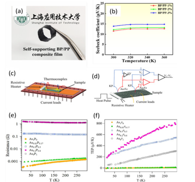
However, according to Xiao et al. [14] As shown in the Figure 2a-2c, BP was utilized as a filler to create flexible self-supporting black phosphorus/PEDOT: PSS (BP/PP) thermoelectric (TE) composite films. These films were created utilizing a solution 3D printing technique, with BP and PP serving as the filler and matrix, respectively. At 360K, a power factor of 13.18μWm-1K-2 was obtained for the BP/PP composite film with a mass content of 2wt.%. The associated electrical conductivity and Seebeck coefficient were 755.53S/cm and 13.21μV/K, respectively. As shown in Figure 2d-2f, Karki et al. [15] have documented the AsxP1−x (x=0, 0.2, 0.5, 0.83, and 1) alloys’ structural and temperature-dependent transport characteristics. Black arsenic-related phonon modes in these samples are observed to blueshift as the phosphorus concentration increases, while black phosphorous-related phonon modes in the sample are observed to redshift as the arsenic concentration increases. At room temperature, it exhibits extremely high thermopower values, rising to 803μV/K for x = 0.2 as illustrate in Figure 2f. Rodrigues et al. [16] have published the bulk BP that was produced at high temperatures and high pressures. The value of thermal conductivity variations between 14.5 and 6.2Wm-1K-1 throughout the 323-673K range, which is lower than the values previously reported for single-crystals.
Figure 2:(a) Digital image of BP/PP composite, (b) Temperature dependent see beck coefficient of the BP/PP, Reproduced with permission from [14], (c) Schematic of the measurement setup, (d) circuit diagram measuring the thermos power with the 4-probe resistance setup, (e) Temperature dependence on 4-probe resistance, (f) output thermopower of Arsenic doped BP for x = 0.2 Reproduced with permission from [15].
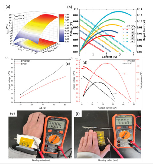
MXene: MXenes can be made by selectively etching the “A” layers with the right hydrofluoric acids, which exfoliates the MAX phases into 2D nanosheets [17]. “M” stands for an early transition metal (Sc, Ti, V, Cr, Zr, Nb, Mo, Hf, Ta), “A” for an element from groups 13-16 of the periodic (Al, Si, P, S, Ga, Ge, As, In, Sn, Tl, Pb), and “X” for carbon and/or nitrogen. When n is 1, 2, or 3, these materials are described as Mn+1AXn. Because of its remarkable thermal stability in air, MXene has been studied as a high-temperature thermoelectric material. Using the developed p-type 1 vol% Ti3C2Tx/BST composite, as illustrated in Figure 3a-3b, Lu et al. [18] provides a homogeneous dispersion of 2D inclusion in matrix. The first evidence is that by incorporating MXene (Ti3C2Tx) into BST (Bi, Sb)2Te3), a record-high thermoelectric conversion efficiency of up to 7.8% is obtained in TE power generation devices under a temperature gradient of 237K. Further the incorporation of two-dimensional Ti3C2Tx MXene into the SnSe matrix through solution synthesis and rapid consolidation, as reported by Zhang et al. [19] effectively raises the carrier mobility and concentration; consequently, the temperature range of 323-523K has increased electrical conductivity. In the interim, at 773K, SnSe/Ti3C2Tx composites provide a low value of 0.41Wm-1K-1, indicating reduced lattice thermal conductivity. After adding 0.3 weight percent Ti3C2Tx, the SnSe/Ti3C2Tx composite finally reaches a peak ZT of 0.93 at 773K, which is 66% higher than that of SnSe. Additionally, Zhang et al. prepared ternary thermoelectric films of PEDOT: PSS/SWCNT/Ti3C2-Cl (PPSCT) by introducing Ti3C2-Cl into poly(3,4-ethylenedioxythiophene): poly (4-styrenesulfonic acid) / single walled carbon nanotubes (PEDOT: PSS/SWCNT, referred to as PPSC) [20].
The microscopic morphology, microstructure, and thermoelectric characteristics of PPSC and PPSCT films demonstrate that the addition of Ti3C2-Cl tends to increase the Seebeck coefficient while decreasing electrical and thermal conductivity. At a temperature differential of 50K, the PPSCT films can generate a maximum output power of 54.36nW and an output voltage of 4.5mV as illustrated in Figure 3c-3f. They are remarkably flexible in producing a sensitive output voltage of 0.6mV between the skin and the environment at a temperature differential of 7K. The electrical conductivity, Seebeck coefficient, and thermal conductivity of PPSCT films reach their optimal values of 1683S/cm, 21.69μV/K, and 14.97W/mK, respectively, when the Ti3C2-Cl content reaches 8 weight percent. The power factor (PF) and thermoelectric figure of merit (ZT) are 79.23μW/mK2 and 1.58×10⁻³, respectively.
Figure 3:(a) 3D plot in order to estimate the maximum conversion efficiency (ηmax), (b) the current dependent output voltage and power curve at various temperature gradient by incorporating MXene (Ti3C2Tx) into BST (Bi, Sb)2Te3), Reproduced with permission from [18], (c) the output voltage PPSC and PPSCT films, (d) output power, and current produced by PPSC and PPSCT films at a 50K temperature difference, (e) the output voltage generated TE device worn on the wrist, and (f) by the hand pressed, Reproduced with permission from [20].
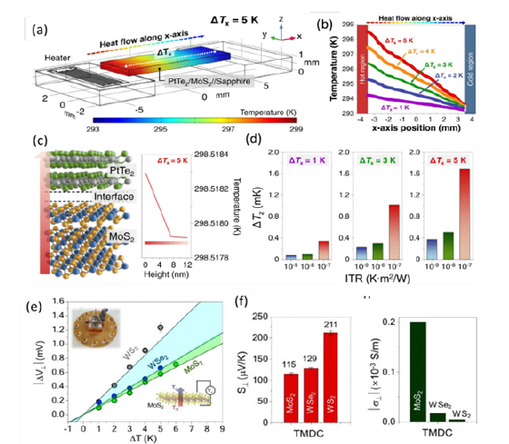
TMDC: Two-dimensional (2D) metal dichalcogenides (TMDCs) including MoS2, MoSe, WS2, and WSe2 are the promising material for TE applications because of their excellent electronic and phonon transport properties, which are made possible by an atomically thin layer that acts as an ideal quantum well structure and a favorable large energy band gap. Using first-principles calculations, Han et al. [21] have concentrated on the thermoelectric characteristics of WS2- WSe2 nanoribbons with superlattice (SL) and Janus (JA) structures. High structural stabilities are demonstrated by WS2, WSe2, SL, and JA nanoribbons with ribbon widths ranging from 5 to 7. Since all nanoribbon electrical structures are semiconductors, bandgaps will change depending on the width of the ribbon. Additionally, it is noted that the greatest carrier mobilities (up to about 500-1400cm2 V−1s−1) and relaxation periods (up to approximately 400-600 fs) are present in nanoribbons with a ribbon width of 5 in WS2, SL, and JA. Additionally, as shown in Figure 4a-4d, Choi et al. [22] develops a novel method for increasing the in-plane TE power factors by piling metallic PtTe2 films on intrinsic MoS2 films with high resistance (>10 MΩ) to use the wet-transfer stacking technique to produce trilayer-PtTe2/MoS2/MoS2 (5nm/7nm)//sapphire and bilayer- PtTe2/MoS2 (5nm/7nm/7nm)//sapphire heterostructures. Such methods can be accomplished by using a metallic high-conductivity top-PtTe2 film in conjunction with a 2D/2D heterostructure to increase the electron effective mass because of the strong electronelectron interaction at the interface and, ultimately, increase Seebeck coefficients via interface-driven Seebeck effect. The Tri layer-stacked PtTe2/MoS2/MoS2 heterostructures have a power factor of around 0.2mW/m⋅K2 and a Seebeck coefficient of -21.6μV/ K, which are 231% and 727 % greater, respectively, than the metallic 5-nm-thick single PtTe2 film on the sapphire substrate. Whereas Kang et al. [23] have analyzed and directly contrasted the crossplane Seebeck coefficients of multiple chemical vapor deposition (TMDC) films. The figure indicates that for MoS2, WSe2, and WS2 thin films, these coefficients are around 115, 129, and 211μV/K at 300K, respectively as demonstrated in Figure 4e-4f. Strong anisotropic behavior with a ratio of around 6.5 along in- and crossplane directions, as well as superior in-plane Seebeck coefficients of approximately 742μV/K, are displayed at 300K by the chemically created holey structure of MoS2 thin films with a thickness of roughly 7nm. Additionally, Yang et al. [24] created a flexible and wearable self-reassembly WTEG using 1T-phase molybdenum disulfide (MoS2) nanosheets as a p-type material and modified TiS2 nanosheets as an n-type material. The generator demonstrated its potential for real-world uses by producing a voltage output of roughly 15mV while collecting heat from the human arm.
Figure 4:(a) the estimated temperature distribution using COMSOL while measuring the see beck coefficient, (b) the temperature profiles corresponding the dotted lines present in (a). (c)he obtained ΔTz from the MoS2 to PtTe2 when the ΔTx =5K, (d) ITR-dependent ΔTz according to the temperature gradient of 1, 3, and 5K, Reproduced with permission from [22] (e) the output voltage for WS2, WSe2, and MoS2 based thin films as a function of ΔT from 1 to 6K. Insets show the schematic of the module, (f) the evaluated Seebeck thermopower and electrical conductivity of the WS2, WSe2, and MoS2 based thin films Reproduced with permission from [23].
Others: Some other 2D materials such as boron nitride have good electronic, optical, and vibrational properties. Whereas the graphite phase carbon nitride (g-C3N4) is nitrogen substituted graphene 2D materials with easy preparation, no toxicity, a low band gap (2.5-2.8eV), and good stability. On the other hand, a lot of work has been done in recent years to improve their thermoelectric qualities. The more electricity produced, the higher the figure of merit (ZT) value. In order to create a multi-phase composite with synergistic thermoelectric and mechanical properties, Cheng et al. [25] have integrated boron nitride (BN) into tin-enriched SnSe2. The addition of BN to SnSe2 has the dual advantage of increasing carrier mobility and concentration. The BN/SnSe2 composite exhibits a notable increase in the Seebeck coefficient, as confirmed by density functional theory simulations.
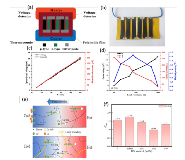
This is attributed to a wider bandgap and electronic density of states around the Fermi level. As demonstrated in Figure 5a-5d, Li et al. [26] produced flexible, free-standing g-C3N4/ SWCNT thermoelectric composite films by vacuum-filtering and mechanically joining g-C3N4 and SWCNTs. The findings show that the interfacial π-π interaction effectively covers g-C3N4 on the surface of SWCNTs, and that a g-C3N4 layer applied to SWCNTs at several nanometers concurrently increases the electrical conductivity (σ) and Seebeck coefficient (S) of g-C3N4/SWCNT. At a mass ratio of 2.5%, g-C3N4/SWCNT achieves an ideal power factor value of 163.0±1.0μW m−1 K−2, with a σ of 702.6±1.6S cm−1 and a S of 48.2±0.2μV K−1 at room temperature. Further as shown in Figure 5e, to improve thermoelectric performance and service stability, Lin et al. [27] integrated hexagonal boron nitride (h-BN) into nano-Cu2−xSe. Due primarily to a notable decrease in lattice thermal conductivity (kL) to almost 50% (0.13W m−1 K−1), it was discovered that Cu2−xSe-0.005 weight percent BN had a higher value of figure of merit (ZT) approximately 1.76, 11% higher than that of pure Cu2− xSe at 923K as shown in Figure 5f. Singh et al. [28] examined the effect of adding carbon nanotubes (CNTs) and g-C3N4 nanosheets on the thermoelectric characteristics of PEDOT: PSS. The Seebeck coefficient increased sharply when g-C3N4 nanosheets were introduced to PEDOT: PSS. At 313K, at a concentration of 10 weight percent g-C3N4 nanosheets, it reached 74.3μVK−1, approximately five times higher than the Seebeck coefficient of the PEDOT: PSS films.
Figure 5:(a) Schematic diagram of the TE device, (b) photograph of the fabricated TE device, (c) output voltage and current in different temperature gradient, (d) Voltage/current and power/current curves ata fix temperature difference of 50K, Reproduced with permission from [26]. (e)schematic representation of Cu+ migration and BN blocking the Cu+ migration in presence of electric field, (f) the estimated figure of merit (ZT) with the varying concentration of BN content. Reproduced with permission from [27].
Conclusion and Outlook
The development of thermoelectric materials has advanced significantly during the past few decades. Since they are new to the thermoelectric material family, 2D materials have garnered a lot of interest and numerous groundbreaking studies have been published. It is anticipated that 2D thermoelectric materials will be the next generation of high-performance thermoelectric materials because of their distinct electrical, thermal, and mechanical characteristics. The thermoelectric characteristics of several 2D materials, including TMDCs, graphene, BP, MXene, and others, as well as their nanocomposites, were thoroughly demonstrated in this review. Furthermore, the most recent theoretical and experimental data were provided to clarify the relationship between the several elements that affect these materials’ thermoelectric characteristics.
These are some major outlooks which need to be address in the
following issue.
a) The ability to effortlessly generate scalable, high-quality
2D content is really crucial. This is an active study issue right
now. To date, a variety of techniques have been used to create
2D materials, including molecular beam epitaxy, chemical vapor
deposition, mechanical exfoliation, atomic layer deposition,
physical vapor deposition liquid exfoliation, and mechanical
exfoliation. However, using scale-up techniques to manufacture
such materials with a regulated structure remains difficult.
b) Although the electrical conductivity of 2D materials is
very promising, their thermal conductivity is higher than that
of conventional semiconductors. It is necessary to address
this constraint. Their structural alterations, the addition of
structural flaws, and the management of their constituent parts
through the creation of composites or other techniques would
all positively affect the thermoelectric performance of the 2D
materials.
c) Another difficult limitation is the creation and
characterization of thin films made of 2D materials. In general,
methods like spin coating, PVD, CVD, and maybe atomic layer
deposition (ALD, which is a more specialized process) can be
used to scale up their manufacturing. The cost-effectiveness of
several of these methods in commercial applications, however,
may be impacted by their strict high vacuum requirements.
Additionally, methods for directly fabricating thin-film
thermoelectric devices are attractive since they can streamline
the fabrication process.
References
- Kanahashi K, Pu J, Takenobu T (2020) 2D materials for large‐area flexible thermoelectric devices. Adv Energy Mater 10(11): 1902842.
- Wang L, Zhang Z, Geng L, Yuan T, Liu Y, et al. (2018) Solution-printable fullerene/TiS2 organic/inorganic hybrids for high-performance flexible n-type thermoelectrics. Energy Environ Sci 11: 1307-1317.
- Yang J, Yip H, Jen AK Y (2013) Rational design of advanced thermoelectric materials. Adv Energy Mater 3: 549-565.
- Biswas K, He J, Blum ID, Wu CI, Hogan TP, et al. (2012) High-performance bulk thermoelectrics with all-scale hierarchical architectures. Nature 489: 414-418.
- Grimme S, Antony J, Ehrlich S, Krieg H (2010) A consistent and accurate ab initio parametrization of density functional dispersion correction (DFT-D) for the 94 elements H-Pu. J Chem Phys 132.
- Lai J, Liu X, Ma J, Wang Q, Zhang K, et al. (2018) Anisotropic broadband photo response of layered type‐II weyl semimetal MoTe2. Advanced Materials 30(22): 1707152.
- Nie C, Yu L, Wei X, Shen J, Lu W, et al. (2017) Ultrafast growth of large-area monolayer MoS2 film via gold foil assistant CVD for a highly sensitive photodetector. Nanotechnology 28(27): 275203.
- Tao W, Kong N, Ji X, Zhang Y, Sharma A, et al. (2019) Emerging two-dimensional monoelemental materials (Xenes) for biomedical applications. Chem Soc Rev 48: 2891-2912.
- Ahmadi S, Raeisi M, Eslami L, Rajabpour A (2021) Thermoelectric characteristics of two-dimensional structures for three different lattice compounds of B-C-N and graphene counterpart BX (X = P, As, and Sb) systems. The Journal of Physical Chemistry C 125: 14525-14537.
- Zhang D, Mao Y, Bai P, Li Q, He W, et al. (2022) Multifunctional superelastic graphene-based thermoelectric sponges for wearable and thermal management devices. Nano Lett 22(8): 3417-3424.
- Khoso NA, Xu G, Xie J, Sun T, Wang J (2021) The fabrication of a graphene and conductive polymer nanocomposite-coated highly flexible and washable woven thermoelectric nanogenerator. Mater Adv 2: 3695-3704.
- Wei T, Li H, Fu Y, Zheng X, Huang L, et al. (2023) A graphene-nanoribbon-based thermoelectric generator. Carbon NY 210: 118053.
- Chien NV, Park HM, Shin H, Song JY (2025) Multiscale defect-assisted enhancement of thermoelectric transport in Sn-doped black phosphorus polycrystals. ACS Omega 10: 15621-15628.
- Xiao C, Liu X, Meng Q, Wang L, Du Y, et al. (2024) Fabrication of flexible self-supporting black phosphorus nanosheet/PEDOT: PSS thermoelectric composite films by solution 3D printing technology. Composites Communications 46: 101815.
- Karki B, Rajapakse M, Sumanasekera GU, Jasinski JB (2020) Structural and thermoelectric properties of black arsenic–phosphorus. ACS Appl Energy Mater 3: 8543-8551.
- Rodrigues JEFS, Gainza J, Serrano-Sánchez F, López C, Dura OJ, et al. (2020) Structural features, anisotropic thermal expansion, and thermoelectric performance in bulk black phosphorus synthesized under high pressure. Inorg Chem 59: 14932-14943.
- Wen C, Liao Q, Cui Z, Chen Z, Liu H, et al. (2023) Exfoliation behavior and superior photothermal conversion performance of MXenes beyond Ti3C2Tx. Chemical Engineering Journal 472: 144921.
- Lu X, Zhang Q, Liao J, Chen H, Fan Y, et al. (2020) High‐efficiency thermoelectric power generation enabled by homogeneous incorporation of MXene in (Bi,Sb)2Te3 Adv Energy Mater 10(2): 1902986.
- Zhang H, Chen Y, Liu X, Wang H, Niu C, et al. (2022) Enhancing the thermoelectric performance of solution-synthesized SnSe-based materials via incorporating Ti3C2T MXene. Mater Today Energy 30: 101137.
- Zhang Y, Zhu C, Chen Y, Wang L, Huang X, et al. (2024) Self-powered PEDOT: PSS/CSWCNT/Mxenes thermoelectric films and wearable electronics devices. Surfaces and Interfaces 50: 104526.
- Han D, Wang M, Yang X, Du M, Cheng L, et al. (2022) Discovery of high thermoelectric performance of WS2-WSe2 nanoribbons with superlattice and Janus structures. J Alloys Compd 903: 163850.
- Choi JW, Lee WY, Kim SH, Kang MS, Cho JM, et al. (2023) Interface-driven see beck effect in two-dimensional trilayer-stacked PtTe2/MoS2/MoS2 heterostructures via electron–electron interactions. Nano Energy 115: 108713.
- Kang MS, Kang SY, Lee WY, Park NW, Kown KC, et al. (2020) Large-scale MoS2 thin films with a chemically formed holey structure for enhanced Seebeck thermopower and their anisotropic properties. J Mater Chem A Mater 8: 8669-8677.
- Yang Y, Huang H (2025) Self-reassembly wearable thermoelectric generator using surface-modified TMDCs. Appl Phys Lett 126.
- Chen Y, Nisar M, Qin W, Xu Z, Danish MH, et al. (2025) Integration of boron nitride into tin‐enriched SnSe2 for a high‐performance thermoelectric nanocomposite with optimized electrical transport and mechanical properties. Adv Funct Mater.
- Li Y, Jiang D, Li Z, Yang Z, Fu P, et al. (2023) High-performance g-C3N4 coated single-walled carbon nanotube composite films for flexible thermoelectric generators. Diam Relat Mater 138: 110225.
- Lin Z, Guo Y, Bai J, Hong A, Li C, et al. (2025) Impact of boron nitride on the thermoelectric properties and service stability of Cu 2-x ACS Appl Mater Interfaces 17: 1922-1930.
- Singh M, Khare N (2024) Enhancing the thermoelectric properties of PEDOT: PSS films through the incorporation of g-C3N4 nanosheets and carbon nanotubes. Composites Communications 51: 102092.
© 2025 Neeraj Dhariwal. This is an open access article distributed under the terms of the Creative Commons Attribution License , which permits unrestricted use, distribution, and build upon your work non-commercially.
 a Creative Commons Attribution 4.0 International License. Based on a work at www.crimsonpublishers.com.
Best viewed in


.jpg)


 Editorial Board Registrations
 Submit your Article
 Refer a Friend
 Advertise With Us
.jpg)


.jpg)


.bmp)
.jpg)
.png)
.jpg)


.jpg)


.png)

.png)


.png)


