
- About Us
- Information
-

The Author ensures that the research has been conducted responsibly and ethically with adherence to all relevant regulations. read more..
- For Authors
- For Reviewer
- Manuscript Guidelines
- Membership
- Publication Ethics
-
- Journals
- Reprints
- e-Books
- Videos
- Policies
- Contact Us
 COVID-19
- Submissions


Full Text
Research & Development in Material Science
IR Transparent Ceramic Microfluidic Chips Produced by Powder Injection Molding
Tao Li1*, Wei Zhai1, Jovyn Neo2, Ngiap Hiang Loh2, Vincent Garland Marc3, Shuying Cheng3, Liang Feng Guo3, Tung Dinh Nguyen3, Ong Nuan Qin3 and Martin Karl Schreyer3
1Singapore Institute of Manufacturing Technology (SIMTech), Singapore
2School of Mechanical and Aerospace Engineering, Nanyang Technological University (NTU), Singapore
3Institute of Chemical and Engineering Science (ICES), Singapore
*Corresponding author: Tao Li, Singapore Institute of Manufacturing Technology (SIMTech), 73 Nanyang Drive, Singapore
Submission: June 28, 2021;Published: July 07, 2021

ISSN: 2576-8840 Volume 15 Issue 3
Abstract
Microfluidics has been broadly employed to analyze chemical/biological processes due to its advantages in fast analysis speed, reduced reagent consumption and enhanced system performance and functionality. Most polymeric and glassy substrates used in microfluidics chips are not transparent in the mid-IR region. Moremore, the normal IR-compatible materials are expensive and challenging for micro-fabrication. Transparent polycrystalline ceramics can solve the problems and have potential to be used in microfluidics applications coupled with FTIR analysis, providing that the required micro-features can be manufactured in the transparent ceramic substrates. Powder Injection Molding (PIM) combining plastic injection molding and conventional powder metallurgy has been applied to produce near-net shape high performance products with small features. In this paper, IR transparent ceramic microfluidic chips with small channel size were produced by PIM process. The feature profile, microstructures and optical properties of the produced parts are characterized.
Introduction
Microfluidics devices have gained tremendous interest in both academic and industrial research due to key advantages such as fast response times and low analytic consumption. Micro-fabrication of microfluidics devices typically involves the use of polymer materials or glass due to the ease of fabrication, low manufacturing costs and the optically transparency of the resulting substrates in the UV/visible part of the electromagnetic spectrum.
Most popular detection methods normally involve optical techniques such as absorption spectroscopy and fluorescence spectroscopy. However, UV and visible absorption methods lack chemical specificity while fluorescence-based methods rely on the existence of a suitable tag that can be attached to the molecule of interest. Additionally, there are significant challenges associated with the detection of small molecules by fluorescence since the properties of a small molecule can be significantly altered by the presence of an extrinsic tag.
Currently, some microfluidics applications are integrated with infrared spectroscopy, which is used to measure the bond vibration frequencies in a molecule and determine the functional group. It also allows collecting spatially resolved chemical information of the measured samples by recording vibrational spectra at known sample positions. Fourier Transform Infrared (FTIR) spectroscopy, despite its relatively low spatial resolution (around 10 micron), provides rich and label-free chemical information about molecular systems. In addition, Raman and infrared microscopy, which are integrated with mapping and/or imaging technology, can simultaneously give both spectral and spatial information in microfluidics applications.
Andrew [1,2] produced a prototype of microfluidics devices integrating with FTIR spectroscopic imaging. The device is manufactured based on the direct printing of polymer onto the surface of an infrared transparent substrate, followed by encapsulation [1,2]. FTIR integrated with microfluidics was also applied for imaging of live cells [3]. Tao et al. [4] demonstrated CaF2 microfluidics devices for maximum flexibility in optical detection, which enable both quantitative and qualitative optical analyses in laboratory-on-a-chip systems [4]. As well, Kelven [5] indicated microfluidics and the future of drug research with drug’s infrared spectrum taken using a technique called ATR-FTIR. The intensity of the signal will give an indication of the concentration of the drug at the point where the microfluidics chip was probed using the spectrometer [5]. Effendi et al. [6] demonstrated rapid assess and map chemical concentration profiles in various regions of a microfluidics device using Raman microscopy combined with band-target entropy minimization analysis (BTEM) [6].
Despite some research of integrating microfluidics application with IR analysis techniques, the major challenge is the production of IR compatible microfluidics chip. The normal polymeric materials for microfluidics applications are often not compatible with organic solvents used in organic syntheses. Those IRcompatible substrates, such as BaF2, CaF2, ZnSe, are quite expensive and challenging for micro-fabrication process. Anisotropic etching of channels in CaF2 has been used by Brynson [7] to fabricate IRtransparent microfluidic devices with strong acid. The application of micro-fabrication concepts for the realization of fluidic devices suitable for the real-time monitoring with IR microprobes is still in its infancy.
Many oxide materials in single crystal form are transparent in UV-visible-IR range and has the potential to be used in microfluidics application coupled with IR analysis techniques. However, the growth and machining of single crystals to form different shapes and features is an expensive task, which largely limits their scale up of production and, therefore, their range of applications. These problems can be solved with the use of transparent polycrystalline materials as they show similar mechanical, chemical and thermal stability compared to single crystals and can be produced in complex shapes and are not size limited as single crystals.
Transparent ceramics can be produced by traditional powder metallurgy route. The green parts formed by die pressing or cold isostatic pressing will be sintered at high temperature with or without pressure to get final pore-free products. However, it is challenging to produce micro-feature for microfluidics application with the traditional methods. Powder injection molding (PIM) is a powder processing technology combining plastic injection molding and conventional powder metallurgy to produce geometrically complex products. As a net or near-net shape process, large volume parts with complex micro features as low as 100μm can be produced by PIM at a relatively low cost. In this paper, the feasibility to produce IR transparent ceramic microfluidic chips produced by PIM is demonstrated.
Experimental
Raw materials
Highly pure yttria (Y2O3) powder purchased from Nippon Yttrium CO., LTD Japan was used as the matrix material in this paper. Figure 1 shows the SEM pictures of the as-purchased powder at low and high magnifications. The powders showing spherical balls with diameter of 30~50μm after spry drying. Each ball is a cluster of sub-micron yttria powders.
Figure 1: SEM of as-purchase powder at low and high magnifications.

The size of the as-purchased powder was analyzed by Laser Scattering Particle Size Distribution Analyzer Particle LA-960 and the result is shown in Figure 2. It can be seen from Figure 2 that the average size of the yttria powder is around 0.25μm after breaking up the spray dried balls.
Figure 2: Yttria powder size distribution.

Many additives have been investigated for preparation of transparent yttria ceramic. In this paper, 5mol% 3Y-zirconia (Tosoh, Japan) was used as an additive to reduce sintering temperature and improve the transparency. An in-house developed binder system based on Paraffin Wax (PW), polypropylene (PP) and Stearic Acid (SA) was used for the PIM process.
Sample preparation
In order to achieve good uniformity, which is one of the key factors affecting the final transparency, wet mixing of yttria powder and zirconia powder by ball milling was carried out before mixing with binder components.
Feedstock with a solid loading of 50vol% was prepared in a double planetary mixer after ball milling of yttria and zirconia. The granulated feedstock went through two rounds of highly shear extrusion with Thermo Scientific Process 11 Twin Screw Extruder to ensure a homogeneous mixture.
Injection molding was carried out with an Arburg 220S 150- 60 injection molding machine. After process optimization, circular discs of Φ20mmx2mm and square microfluidic chips of 25mm x 25mm x 2.5mm with micro-channels of width 200μm and depth of 100μm was produced as shown in Figure 3.
Figure 3: Green parts of a) circular discs and b) microfluidic chips.

Solvent debinding combined thermal debinding was used to remove the binder components in the green parts. In the solvent debinding, the green parts were immersed in hot solvent to remove most of the PW and SA. The remaining binder was removed in a multi-stage thermal debinding process, in which the parts were heated up in an inert atmosphere and strictly controlled heating profile.
After thermal debinding, the brown parts were transferred to an all-metal high vacuum furnace (Thermal Technology LLC Sintering Furnace, USA) to carry out the sintering process at temperature of 1770 °C and different dwell durations.
Characterization
The sintered parts were characterized in terms of dimension, microstructure, phases and transmittance. The depth and width of the micro-channels were measured using the PLu Sensorfar Confocal Imaging Profiler. The microstructure of the specimen was examined using Scanning Electron Microscope (SEM) after grinding, polishing and thermal etching. The phases presented in the sintered parts were examined by X-ray Diffraction (XRD). The transmittance of the specimen was quantified using UV/VIS/NIR spectrometer with a wavelength range from 400nm to 2200nm.
Result and Discussion
Effect of zirconia additive
The zirconia additive plays a critical role in manufacturing transparent yttria as shown in Figure 4, in which the discs were sintered at 1750 °C without and with zirconia addition. It is clear that the as-sintered sample without zirconia addition (Figure 4a) is still opaque while certain transparency has been achieved with zirconia addition in the as-sintered disc (Figure 4a).
Figure 4: As sintered yttria discs a) without and b) with zirconia additve.

Figure 5 shows the microstructure of the above two samples after thermal etching. It is well known that porosity is the most significant factor affecting the ceramic materials’ transparency. The boundary of the residual pores will reflect and refract light intensely due to sharply different optical properties, leading to opaque ceramics. It can be seen from Figure 5a that many residual pores still remained in the sintered yttria sample without zirconia addition. In contrast, almost fully dense microstructure is observed in the sample with zirconia addition (Figure 5b), making it more transparent. Figure 5 also shows that the grain size in pure yttria sample is bigger than that of sample with zirconia addition.
Figure 5: Microstructure of sintered yttria samples a) without and b) with zirconia additve.

It is generally believed that segregation of zirconia at the grain boundaries will suppress matrix’s grain growth and enhance densification. In this work, the phases presented in the zirconia doped yttria samples before and after sintering were analyzed by XRD and the results are shown in Figure 6. The XRD result clearly shows two phases, namely zirconia (7.54wt%) and yttria (92.4wt%), in the sample before sintering (Figure 6a). The percentage of two materials are aligned to the initial mixture. However, the XRD test on the sintered sample only shows peaks of yttria phase (Figure 6b). No zirconia and other compounds can be identified from the result.
Figure 6: XRD analysis of zirconia doped yttria samples a) before and b) after sintering

Detailed study of the XRD result of sintered yttria sample and compared with the standard XRD peaks, it can be found that an extra small peak appears near the yttria’s (222) peak (red circle in Figure 6b. Such extra peak is normally caused by lattice distortion of the matrix material. This lattice distortion can be induced by introduction of second atoms with different sizes. In this zirconia doped yttria, it is believed that solid solution is formed at high sintering temperature based on the following reaction:
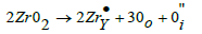
In this solid solution, position of Y atom is replaced by Zr atom because of similar atom size. With two Zr atoms replacing Y atoms, one O interstitial is produced to maintain charge balance and leading to lattice distortion. The lattice distortion in the grains may decrease atom diffusion and grain boundary mobility. Therefore, the yttria grain growth is inhibited by zirconia addition; smaller grain size, higher density and transparency can be obtained with no residual pores entrapped inside the grains.
Transmittance of sintered parts
Figure 7 shows the polished yttria disc sample with zirconia additive, showing better transparency compared with the assintered part shown in Figure 4b.
Figure 7: Polished yttria ceramic disc.

Light transmittance was measured from a wavelength of 380nm to 2500nm on the as sintered and polished sintered part as shown in Figure 8. It can be seen from Figure 8 that there is around 10~20% increase in light transmittance from the un-polished sample to the polished sample. This is due to less light being scattered at the polished surface compared to that of the un-polished surface. For the part after polishing, the transmittance is around 50-70% in the visible light range (400-800nm). The transmittances increase from short wavelength to long wavelength and the sample has a transmittance of 70-74% at the infrared wavelength. Compared with yttria single crystal, which has a transmittance around 80% in the same wavelength range [8], ninety percent of transmittance can be achieved in the polycrystalline ceramic produced by powder injection molding.
Figure 8: Light transmittance of sintered yttria ceramic disc.

Profile of microfluidics channels
The as sintered yttria ceramic microfluidics chip is shown in Figure 9. The transparency of the part is not dramatically affected by the micro channels. Figure 10 shows the top view and cross section of the channel under optical microscope with width of around 250μm and depth of around 90μm.
Figure 9: As-sintered microfluidics chip.

Figure 10: Micro-channel in the sintered chip from a) top view and b) cross section.

The depth and width of channels were measured using a PLu Sensorfar Confocal Imaging Profiler. Figure 11 shows the 3D construction of the micro-channels in the sintered part and Figure 12 shows the measurement of green parts and sintered parts. It can be seen that the width of channel was decreased from 320μm in the green part to 230μm in the sintered part, while the depth decreased from 115μm to 85μm. The sintering shrinkage factor is around 26~28%.
Figure 11: 3D construction of micro-channels in the sintered part.

Figure 12: Channel depth and width of the a) green and b) sintered parts.

Conclusion
In this paper, the feasibility of producing IR transparent yttria ceramic microfluidics chip by powder injection molding and vacuum sintering has been demonstrated to cater to some microfluidics applications integrated with infrared spectroscopy. The additive of zirconia into yttria plays a critical role in achieving high density and transparency by forming solid solution and decreasing grain boundary mobility with lattice distortion. The transmittance of yttria disc produced by PIM is around 70%, which is 90% of yttria single crystal. With PIM process, micro-channels with width of 230μm and depth of 85μm can be produced in the sintered ceramic chip.
References
- Andrew Chan KL, Niu X, Mello AJ, Kazarian SG (2010) Rapid prototyping of microfluidics devices for integrating with FT-IR spectroscopic imaging. Lab Chip 10: 2170-2174.
- Andrew Chan KL, Gulati S, Edel JB, Mello AJ, Kazarian SG (2009) Chemical imaging of microfluidics flows using ATR-FTIR spectroscopy. Lab Chip 9: 2909-2913.
- Dougan JA, Kazarian SG (2013) Fourier transform infrared spectroscopic imaging of live cells. Spectroscopy Europe 25(5): 6.
- Pan T, Kelly RT, Asplund MC, Woolley AT (2004) Fabrication of calcium fluoride capillary electrophoresis microdevices for on-chip infrared detection. Journal of Chromatography A 1027(1-2): 231-235.
- Chen K (2011) Microfluidics and the future of drug research. Journal of Undergraduate Life Science 5(1): 66.
- Widjaja E, Teh SY, Garland M (2012) Characterizing diffusion and transport in microfluidics channels: A combined raman microscopy and band-target entropy minimization study. Applied Spectroscopy 66(10): 1226-1232.
- Lehmkuhl B, Noblitt SD, Krummel AT, Henry CS (2015) Fabrication of IR-transparent microfluidic devices b anisotropic etching of channels in CaF2. Lab Chip 15(22): 4364-4368.
- Lakshmanan A (2012) Sintering of ceramics-new emerging techniques.
© 2021 Tao Li. This is an open access article distributed under the terms of the Creative Commons Attribution License , which permits unrestricted use, distribution, and build upon your work non-commercially.
Editor In Chief


.jpg)


Signup for Newsletter

Quick Links
 Editorial Board Registrations
 Submit your Article
 Refer a Friend
 Advertise With Us
Our Recent Edition

.jpg)


Top Editors


.jpg)


.bmp)
.jpg)
.png)
.jpg)


.jpg)


.png)

.png)


.png)


Financial Support

Sponsors

Latest e-Books

Latest Video

 a Creative Commons Attribution 4.0 International License. Based on a work at www.crimsonpublishers.com.
Best viewed in
a Creative Commons Attribution 4.0 International License. Based on a work at www.crimsonpublishers.com.
Best viewed in