
- About Us
- Information
-

The Author ensures that the research has been conducted responsibly and ethically with adherence to all relevant regulations. read more..
- For Authors
- For Reviewer
- Manuscript Guidelines
- Membership
- Publication Ethics
-
- Journals
- Reprints
- e-Books
- Videos
- Policies
- Contact Us
 COVID-19
- Submissions


Full Text
Research & Development in Material Science
Room Temperature Photoluminescence and Optical Parameters of Micro Rods ZnO Thin Films Deposited on Silicon Substrates
Hassan K Juwhari1*, Bashar Lahlouh1 and Shadia J Ikhmayies2
1Department of Physics, University of Jordan, Jordan
2Physics Department, Al Isra University, Jordan
*Corresponding author: Hassan K Juwhari, Department of Physics, University of Jordan, Jordan
Submission: February 06, 2020;Published: February 25, 2020

ISSN: 2576-8840 Volume 12 Issue 5
Abstract
Micro structured zinc oxide (ZnO) is of potential use in solar cells, solid state gas sensors, and other optoelectronic devices. For the advancement of these technologies, a comprehensive understanding of these materials’ optical characteristics is considered essential. Using the spray pyrolysis (SP) method, thin films of ZnO micro rods are deposited from aqueous zinc chloride solution on silicon substrates held at 350±5 °C. The films have been studied using the data acquired from the X-ray diffraction (XRD), scanning electron microscopy (SEM), X-ray energy dispersive spectroscopy (EDS), reflectance and photoluminescence (PL) spectroscopy. Hence, the XRD and SEM confirmed the films’ hexagonal phase and revealed the tapered ends of the hexagonal rods. The optical parameters including the refractive index, extinction coefficient, absorption coefficient, real and imaginary dielectric constants, conductivity, and the energy loss are all deduced from the reflectance spectra. Finally, the photoluminescence spectra of the studied samples are measured at room temperature using two excitation wavelengths: 300 and 365nm. As such, the obtained results confirmed the quality of the prepared films and allowed proper determination of their respective optical characteristics.
Keywords: ZnO micro rods; Optical parameters; Spray pyrolysis; Solar cells; Photoluminescence
Introduction
Zinc oxide is a multipurpose material, which assumes the Wurtzite structure with space group C6v4 or P63mc [1,2]. It is redeemed useful in so many applications including solar cells, solid state gas sensors, photovoltaic and other optoelectronic devices, and in the biomedical industry as well [3-6].
Although numerous preparation techniques including sol-gel [7], electrodeposition [8], hydrothermal [9], chemical bath deposition (CBD) [10], solvothermal synthesis [11], RF sputtering [12], glaze firing [13], reactive sputtering [14], and many others are considered adequate to produce ZnO in its intended thin film forms, the spray pyrolysis in particular has received recently adequate attention because of its simplicity, economics, and ease of scale up for large scale production [15-20]. In addition, the spray pyrolysis method can be easily altered to produce films of different morphologies including nano-sheets, -wires, -combs, -flowers, and -rods [6]. This happens as a direct consequence of the preparation methods and conditions and usually affected by the preferential growth along the c-direction [1,6].
Even though ZnO occurs in nature as an n-type with large exciton binding energy of 60meV and wide bandgap energy of 3.37eV at room temperature [21], it can nowadays be easily synthesized in either n- or p-type by intentionally doping it with elements of group- III or group-I and V, respectively. Nevertheless, its brilliant electrical conductivity is a direct consequence of the zinc excess at the interstitial positions and/or due to the oxygen vacancies [17]. In a previous work, the authors studied the functionalities, compositional quality, and the chemical bonding of the ZnO thin films using FTIR spectroscopy. They observed the Zn-O bond stretching vibration peaks at 420cm-1, 454cm-1, 485cm-1, and 546cm-1, and the substrate’s Si-O stretching vibration at around 1072cm-1 as well [16].
In this work, the authors extend their previous studies to explore in more details both the optical parameters of the prepared ZnO thin films and their room temperature photoluminescence spectra. Both the optical parameters, as deduced from the reflectance spectra, and the measured PL are considered major contributors to the quality of the prepared films and help in providing proper understanding of the films’ optical characteristics that are needed to improve their usage in the optoelectronic industries.
Experimental Procedure
Thin films of ZnO were prepared, using the spray pyrolysis method, on silicon substrates at a substrate temperature of 350±5 ºC. The single-side polished, boron-doped p-type, 3-30Ω cm with (001) orientation, 675±25μm thick Si substrates of area of 5×5mm2 were cut from a 150mm wafer (Semiconductor Wafer, Inc.). Prior to heating the substrates in preparation for the deposition process, the wafers were washed with acetone, methanol, DI water, and blown dry. The full preparation protocol is published elsewhere [16]. X-ray diffraction patterns were measured utilizing a Shimadzu diffractometer (Model 7000). The thin films were examined by an FEI scanning electron microscope (Inspect F50) equipped with a Bruker EDS attachment. The room temperature optical reflectance is measured at normal incidence in the wavelength range 240-840nm using the FilmTek-3000 characterization tool. The measured data is later fitted using various models while the films’ thicknesses are given as byproducts of the fits. Hence, the thicknesses of films 1 and 2 are found ~ (200 and 120) nm, respectively. Subsequently, each film reflectance was used to deduce the thin film’s optical parameters including the refractive index, extinction coefficient, absorption coefficient, real and imaginary dielectric constants, conductivity, and the energy loss. Finally, PL spectra at room temperature were recorded with a Cary Eclipse (Varian) Spectrofluorometer under excitation wavelengths of 300 and 365nm. While the spectral monochromator emission slit was kept at 5nm, the excitation slit was opened at 5, 10, or 20nm. For the excitation wavelength 300nm, the PL data was recorded within the range 330-570nm, while for the excitation wavelength 365nm, the PL data was recorded at 390-670nm.
Results and Discussion
The X-ray patterns of the thin films of ZnO deposited by the spray pyrolysis agree well with the reference pattern in the Joint Committee on Powder Diffraction Standards data base (JCPDS card 00-036-1451) as no extraneous diffraction peaks appeared, indicating a phase-pure Wurtzite structure [16]. Calculation of unit cell parameters from the diffraction pattern gave values of ao= (3.2657 and 3.2659±0.0061) Å and co= (5.213 and 5.210±0.057) Å compared with the values of ao= 3.249Å and co= 5.206Å reported by McMurdie et al. [22] SEM images confirmed the hexagonal microrods nature of the well faceted crystals, in a range of particle sizes of much less than 1μm and the Films’ composition from EDSanalysis found to consist of Zn and O mainly in addition to small concentration of Cl [16].
From the reflectance (R) of the two ZnO thin films deposited on silicon substrates as a function of radiation wavelength, measured and published elsewhere [16], it appeared that R decreases as the wavelength of the incident radiation increases with two pronounced maxima. These maxima are the same as observed in the reflectance of a bare Si native oxide. The appearance of these two maxima is due to the very thin layer (~10 - 15 Å) of the native silicon oxide formed on the top of the silicon substrates (SiOx: x ≈ 1.5). However, the direct influence of the ZnO layers on the overall reflectance of the samples is obvious in lowering the reflectance values based on the different thicknesses of the two samples.
The transmittance T was calculated from the reflectance using the relation: 𝑇+𝑅=1, then used to find the absorption coefficient α, where
α = −lnT / t (1)
Figure 1: (a) Alpha of the two ZnO thin films deposited on Si substrates. (b) Exploded view of Sample 1.

Where 𝑡 representing the thickness of each film. (Figure 1a & 1b) depict the relationship between 𝛼 and the photon’s energy hυ(eV). As the figures show, there is a slight increase of 𝛼 with hυ, however the absorption in sample 1 is much greater compared to sample 2 as it is the thicker one. The two maxima related to SiOx are apparent in the curve of sample 2 while they are very weak in sample 1.
To find the refractive index and extinction coefficient of the studied samples, the following relationships are utilized for a light wave incident normally from the air on the films 19.:
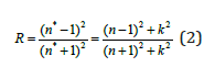
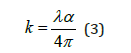
With n* = n + i k, where n is the refractive index and k is the extinction coefficient of the film which also can be calculated using the following relationship based on the absorption coefficient α and the radiation wavelength λ in free space:
Moreover, solving equation (2) for the refractive index gives:
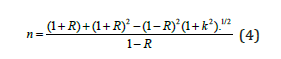
Calculated n and k as a functions of photon’s energy hυ and based on the previous equations were shown in Figure 2 & 3, respectively. Refractive index n, as seen in Figure 2 increases with photons energy, and it is larger for sample 2, which has the smaller thickness. Also, the maxima characteristics of bare Si native oxide are apparent in the curves. Extinction coefficient k decreases with hυ and reaches about 0.4 for sample 1 (the thicker), and 0.9 for sample 2 (the thinner). The non-zero value of k, is due to impurities in the samples. It is observed that k is larger for sample 1, where the larger thickness results in more absorption.
Figure 2: Refractive indices of the two ZnO thin films deposited on Si substrates.

Figure 3: Extinction coefficient of the two ZnO thin films deposited on Si substrates.

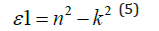
Polarizabilities of solids are related to their dielectric constants where any interaction between the photons and the electrons within the films are reasonably reflected by the variation of the dielectric constants with the photons’ energies. Both real and imaginary components of the complex dielectric constant can be expressed conveniently as given in equations 4 and 5, respectively:
And
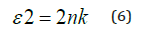
Figure 4 displays how e1 varies with the photon’s energy hυ for ZnO. As shown in the Figure, e1 increases slowly with hυ with two obvious humps. This abrupt increase indicates strong interaction of photons and electrons with maxima at these two energies. Figure 5 displays the imaginary part of the dielectric constant e2 as a function of the photon’s energy hυ for the ZnO film. It is noticeable that e2 behaves exactly like k as it reflects the free carriers’ absorption. The two maxima in e2 occur at the same photons’ energy as in e1. Heating the dielectric material in a varying electric field results in an energy loss which is normally represented by the following relationship:
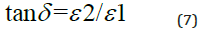
and the loss angle is given as:
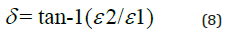
Figure 4: The real part of the dielectric constant 1 against the photon’s energy hυ for the ZnO thin film deposited on Si substrate.

Figure 5: The imaginary part of the dielectric constant 2 against the photon’s energy hυ for the ZnO thin film deposited on Si substrate.

Figure 6: The energy loss as a function of the photon’s energy hυ for the ZnO thin film deposited on Si substrate.

Figure 6 illustrates the relationship between tan δ and hυ for the ZnO film. From the figure, it is shown that the dielectric loss possesses one maximum. The optical conductivity σ of the ZnO thin films can be determined using the formula:
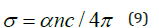
where c represents the speed of light. Projecting the previous formula on the acquired data resulted in obvious variations in the optical conductivity as a function of the photon’s energy hυ and reveals increasing optical conductivity at two maxima along the high energy side that can be attributed to the films’ high absorbance within these regions. Finally, as indicated in all figures, ZnO films of varying thicknesses prepared in this investigation have optical parameters with same features however with different values.
Room temperature characteristic photoluminescence of the deposited films were shown in Figure 7. As shown in Figure 7a & 7b, two main features were seen in the photoluminescence spectra; featured band in the UV region characteristic of the ZnO, and another emission feature extending in the visible region and originating from all sorts of defects and impurities [1,22]. Opening the slit width resulted in higher registered relative intensity as more energy is allowed to excite the luminescent centers within the matrix. Attempts to explain the PL spectra suggests that the UV luminescence is originated from near band edge transitions. The presence of several peaks within the UV region is considered a confirmation indicator of the presence of different nano particle sizes within the films that experience ZnO nanocrystalline excitonic emission (EE) with quantum confinement effects. Moreover, extrinsic impurities as well as deep levels and defects in ZnO crystal structure (i.e. oxygen and zinc interstitials and oxygen and zinc vacancies) are considered mainly responsible for the visible part of the emission spectrum. The zinc interstitials and zinc vacancies (Zni ,VZn) are related to blue emission. The singly ionized oxygen vacancies are commonly attributed to initiate the green emission as it is easily influenced by surface modification. Both orange and green photoluminescence are related to the existing amount of oxygen in the films not to the dopants’ trace amounts [1,4,16].
Figure 7: RT-PL spectra of ZnO thin films for excitation wavelength (a) 365nm. and (b) 300nm. Ex slit width = 5, 10, and 20nm, Em Slit width = 5nm.

Conclusion
Thin films of ZnO were produced on silicon substrates held at 350±5 °C. XRD diffraction revealed the hexagonal structure of the films. SEM microscopy confirmed the hexagonal phase and revealed the morphology of the films, where they showed hexagonal micro rods. EDS, reflectance, and PL measurements were collectively utilized to characterize the films. Optical parameters including α, n, k, e1, e2, σ and the energy loss are all determined based on the reflectance spectra. Measured Room temperature PL spectra presented two featured bands in the UV and visible regions. It is found that varying the thickness of the samples and the presence of impurities have significant effect on the results. The widely opened excitation slits produced the PL of maximum intensity. The measured PL signals consist of UV and VIS luminescence This study is of great interest to photovoltaics’, gas sensors’, and optoelectronics’ industries.
Acknowledgment
The authors acknowledge the financial support of the Deanship of the Academic Research at the University of Jordan. Also, they would like to thank Yousef Abu Salha and Waddah Fares (from The University of Jordan) for their technical assistance in the XRD and SEM data collection.
References
- Juwhari HK, Lahlouh B, and Ikhmayies S (2016) Room temperature photoluminescence of spray-deposited ZnO thin films on glass substrates. Int J Hydrogen Energy 42(28): 17741-17747.
- Juwhari HK, Zihlif A, Elimat Z, Ragosta G (2015) A study on the DC-electrical and thermal conductivities of epoxy/ZnO composites doped with carbon black. Rad Eff Def Solid 169(6): 560-
- Akimov K, Salamov G, Newton JD (2001) Solar cells from past to future. 4th Int, Euresian Congress, Istanbul, Turkey.
- AlDamen MA, Charef N, Juwhari HK, Sweidan K, Mubarak MS, et al. (2016) Crystal structures, optical properties, and TD-DFT study of a zinc (II) schiff-base complex derived from salicylaldehyde and N1-(3-aminopropyl) propane-1, 3-Diamine. J Chem Crystallogr 6(10-12): 411-420.
- Ong CB, Ng LY, Mohammad AW (2018) A review of ZnO nanoparticles as solar photocatalysts: Synthesis, mechanisms and applications. Renewable and Sustainable Energy Reviews 81: 536-
- Oprea O, Andronescu E, Ficai D, Ficai A, Oktar F, et al. (2014) ZnO applications and challenges. Current Organic Chemistry 18(2): 192-
- Mahdavi R, Ashraf TSS (2017) The effect of ultrasonic irradiation on the structure, morphology and photocatalytic performance of ZnO nanoparticles by sol-gel method. Ultrasonics Sonochemistry 39: 504-510.
- Nouri A, Beniaiche A, Soucase BM, Guessas H, Azizi A (2017) Photoluminescence study of Eu+3 doped ZnO nanocolumns prepared by electrodeposition method. Optik 139: 104-110.
- Murillo G, Lozano H, Cases-Utrera J, Lee M, Esteve J (2017) Improving morphological quality and uniformity of hydrothermally grown ZnO nanowires by surface activation of catalyst layer. Nanoscale Research Letters 12(1): 51.
- Husham M, Hamidon MN, Paiman S, Abuelsamen AA, Farhat OF, et al. (2017) Synthesis of ZnO nanorods by microwave-assisted chemical-bath deposition for highly sensitive self-powered UV detection application. Sensors and Actuators A: Physical 263: 166-173.
- Subalakshmi K, Senthilselvan J, Kumar KA, Kumar SA, Pandurangan A (2017) Solvothermal synthesis of hexagonal pyramidal and bifrustum shaped ZnO nanocrystals: natural betacyanin dye and organic Eosin Y dye sensitized DSSC efficiency, electron transport, recombination dynamics and solar photodegradation investigations. Journal of Materials Science: Materials in Electronics 28: 15565-15595.
- Muchuweni E, Sathiaraj TS, Nyakotyo H (2017) Low temperature synthesis of ZnO nanowires on GAZO thin films annealed at different temperatures for solar cell application. Materials Science in Semiconductor Processing 68: 80-86.
- Pekkan K, Taşçi E, Gün Y (2015) The effect of ZnO on development of crystals in crystal glaze applications. Journal of the Faculty of Engineering and Architecture of Gazi University 30(2): 281-287.
- Chabane L, Zebbar N, Trari M, Kechouane M (2017) Opto-capacitive study of n-ZnO/p-Si heterojunctions elaborated by reactive sputtering method: Solar cell applications. Thin Solid Films 636: 419-424.
- Studenikin SA, Golego N, Cocivera M (1998) Optical and electrical properties of undoped ZnO films grown by spray pyrolysis of zinc nitrate solution. J Appl Phys 83: 2104-
- Lahlouh B, Ikhmayies SJ, Juwhari HK (2018) Structural, optical and vibrational properties of ZnO microrods deposited on silicon substrates. J Electron Mater 47(8): 4455-4462.
- Ikhmayies SJ, Abu El-Haija NM, Ahmad-Bitar RN (2010) The influence of annealing in nitrogen atmosphere on the electrical, optical and structural properties of spray-deposited ZnO thin films. Fluid Dyn Mater Process 6: 219-
- Ergin B, Ketenci E, Atay F (2009) Characterization of ZnO films obtained by ultrasonic spray pyrolysis technique. Int J Hydrogen Energy 34(12): 5249-
- Ikhmayies SJ, Zbib MB (2017) Synthesis of ZnO hexagonal micro discs on glass substrates using the spray pyrolysis technique. J Electron Mater 46(7): 3982-3986.
- Lee SH, Lee JS, Ko WB, Sohn JI, Cha SN, et al. (2012) Photoluminescence analysis of energy level on Li-Doped ZnO nanowires grown by a hydrothermal method. Appl Phys Express 5: 095002.
- Singh N, Kumari B, Sharma S, Chaudhary S, Upadhyay S, et al. (2014) Electrodeposition and sol-gel derived nanocrystalline N-ZnO thin films for photoelectrochemical splitting of water: Exploring the role of microstructure. Renew Energy J 69: 242-252.
- McMurdie HF, Morris M, Evans E, Paretzkin B, Wong-Ng W, et al. (1996) Powder Diffr 1:
© 2020 Hassan K Juwhari. This is an open access article distributed under the terms of the Creative Commons Attribution License , which permits unrestricted use, distribution, and build upon your work non-commercially.
Editor In Chief


.jpg)


Signup for Newsletter

Quick Links
 Editorial Board Registrations
 Submit your Article
 Refer a Friend
 Advertise With Us
Our Recent Edition

.jpg)


Top Editors


.jpg)


.bmp)
.jpg)
.png)
.jpg)


.jpg)


.png)

.png)


.png)


Financial Support

Sponsors

Latest e-Books

Latest Video

 a Creative Commons Attribution 4.0 International License. Based on a work at www.crimsonpublishers.com.
Best viewed in
a Creative Commons Attribution 4.0 International License. Based on a work at www.crimsonpublishers.com.
Best viewed in