- Submissions

Full Text
Research & Development in Material Science
Lead-Free Solder Pull-Off Stress Comparison of a Novel Bump Pull Method with Conventional Hot/Cold Bump Pull Methods
Gregory A Turner and DML Meyer*
Department of Mechanical Engineering, The University of Rhode Island, USA
*Corresponding author: DML Meyer, Thermomechanics Laboratory, The University of Rhode Island, Kingston, RI 02881, USA
Submission: April 27, 2018; Published: July 02, 2018

ISSN: 2576-8840 Volume6 Issue5
Abstract
A novel method for directly testing the adhesion strength of three lead-free solders was developed and compared with conventional methods. The Isotraction Bump Pull method utilizes a combination of favorable qualities of the Cold and Hot Bump Pull tests. Solder bumps were generated onto copper printed circuit board substrates using an in-house-fabricated solder bump-on-demand generator. The method uses polymer epoxy to encapsulate solder bumps under uniform tractions, and tested under tension for pull-off stresses. Maximum pull-off stresses for the novel method are: 18MPa (Sn-3.5Ag), 16MPa (SAC 305) and 22MPa (Sn-0.7Cu) and fall at the low end in the literature comparisons. It is suggested that since the copper substrates used in the current work were untreated, that the lower pull-off stress values resulted. Energy Dispersive X-Ray Spectrometry of the newly created faces after fracture shows that brittle fracture of the Intermetallic Compound layer was the mode of failure.
Keywords: Cold bump pull (CBP); Hot bump pull (HBP); Lead-free; Solder; Pull-off stress; Intermetallic Compound (IMC)
Introduction
In years past, tin-lead alloys were used to solder together electrical components. However, health concerns arose from issues surrounding the use and disposal of heavy metals such as lead. After the passing of the Lead Exposure Reduction Act in 1993 in the U.S., and the European Union’s ban of lead in electronics taking effect in 2006, suitable alternatives for tin-lead solders have been pursued [1]. Extensive studies exist of the material properties of lead-free (LF) solders and their fluxes [2-11]. As use of LF solders increases worldwide, the need to create, test, and validate the properties of these solder alloys also has risen.
The requirements of LF solders are much the same as traditional leaded solders; they must have similar melting temperatures, strength and durability, ductility, thermal fatigue resistance, electrical resistance, should use the same manufacturing processes wherever possible, and allow for the continued miniaturization of the electronics industry.
Numerous studies into the mechanical and thermal behavior of these alloys have been conducted in the past few decades, making it possible for the development of industry standards and best practice methods to become available [12-15]. Some of these are the drop impact test, bending test, hot bump pull (HBP), and the cold bump pull (CBP) testing methods.
As the Intermetallic Compound (IMC) layer is known to be the weak location of most soldered joints due to its brittle nature, it is of specific importance to be able to study and quantify the mechanical properties and behavior of IMCs for different LF solders. Taking a focused look into two of the more popular direct solder bump testing methods HBP and CBP, some issues become clear with the study of IMC layers.
Through the insertion of the pin for the HBP method, the solder bumps undergo a large degree of structural change, where both the micro and macro structure of the bump is altered. The addition of the pin also generates a secondary IMC and can cause the characteristics of the first IMC to change due to the reflow that occurs during the insertion process. Despite the CBP method alleviating the need to heat the solder, the clamping process used to gain a mechanical grip upon the exterior of the bump can cause irreversible, plastic deformation to the bump. This deformation has been shown to cause a bias towards brittle fracture and so the associated variables to the process must be optimized through a trial and error process [16]. The added issue to this is then that whenever a new solder, bump size or gripping system is used the variables that were previously optimized can once again become suspect. In order to overcome the issues associated with the HBP and CBP testing methods, and yet still combine their respective positive features while maintaining a direct tensile testing method of solder bumps, a novel method was developed and evaluated: the Isotraction Bump Pull (IBP).
Methodology
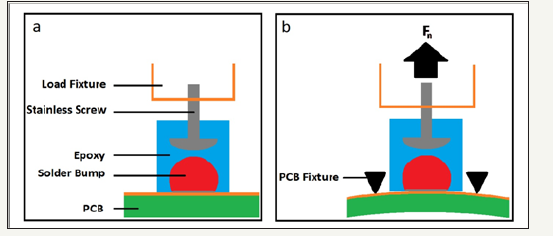
By combining the basic methods of the HBP and CBP testing, it becomes possible to pool positive attributes from both methods. This IBP method, schematically shown in Figure 1, uses a stainless steel screw to replace the hot metal pin of the HBP. However, the pin is not inserted into the bump; rather the screw and bump are encapsulated in a stiff epoxy that is used to transfer the pulling force from the vertical load system to apply uniform tractions over the entire bump surface. This exterior support of the bump resembles the method of the CBP, however there is no need to plastically deform the solder bumps prior to testing to achieve a mechanical grip, as the cast epoxy conforms to the contours of the bump and creates a uniformly secure grip. This lack of plastic deformation of the bump prior to testing not only removes the independent variables associated with the tweezers and clamping process of the CBP, but also does not create the micro-cracks associated with CBP that both weaken the bumps and can cause a bias towards brittle fracture.
Figure 1:Isotraction Bump Pull (IBP) diagram (a) Assembly (b) Testing.
In order to allow for this method to be used on existing equipment commonly in practice for the HBP and CBP, a pulling speed of 0.3mm/s was used. Additionally, the printed circuit board (PCB) substrates used in this study were held in place from the beginning of the test and not allowed a ramp-up run to reach the set speed of the system.
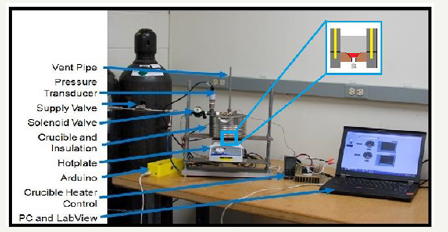
The bumps in this study were generated from three types of LF solder to evaluate the method’s universal application, namely Sn- 3.5Ag, Sn-3.0Ag-0.5Cu, and Sn-0.7Cu, referred to hereafter as SnAg, SAC305 and SnCu, and were created using a bump-on-demand generator, as seen in Figure 2. The generator was designed based on the works of several authors in the literature with slight alterations [17-20]. By changing the magnitude and duration of pressure pulses of nitrogen gas used to generate each bump, the size of the solder bumps could be increased or decreased as desired without any mechanical changes to the system. Also, the bumps for the Sn-3.5Ag alloy were generated first, to eliminate any cross-contamination of these bumps with the copper contained in the other two solder alloys. The bumps had an average mass of 150mg, ±20mg.
Figure 2:Bump on demand generator.
In order to cast the epoxy around the solder bumps and encapsulate both the solder and stainless steel screws, a custom epoxy molding form was designed and fabricated. This system, shown in Figure 3, was composed of an aluminum base plate used to position six individual PCB substrates with the corresponding bumps into the middle of circular Teflon (PTFE) molds, cut from tubular sections of pipe with an outside diameter of 25.4mm and an inside diameter of 12.7mm.
Figure 3:Epoxy casting assembly (a) Assembled (b) Disassembled.

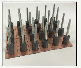
To allow for the mold forms to be removed after casting, the tube sections were cut in half vertically. There were no cleaning processes, deoxidizing or fluxing processes used on the copper substrates. Each substrate was positioned in the machined base plate of the casting mold. The Teflon forms were positioned around the individual bumps and PVC sheets with machined corresponding notches to the forms were bolted onto the bottom plate. A top plate of transparent polycarbonate plastic was used to allow visual inspection of the interior of the casting molds. A throughhole was made in this top plate at the corresponding center positions of each of the six casing forms. These holes allowed for the positioning of the stainless steel screws that would function as the pins for the tensile tests. The mold casting components were assembled with the PCBs and bumps, forms, and pressure plates. Then two-part epoxy (JB Weld, Sulphur Springs, TX) was cast into the forms individually. Immediately after the epoxy was cast, the top plate was used to position the stainless steel screws in place and ensure that the forms were fully seated on the face of the PCB substrates. The system was put under pressure using through bolts from the bottom aluminum to the top polycarbonate plates and the epoxy was allowed to cure for 18 hours, per the manufacturer’s recommendations. At the completion of this process, shown in Figure 4, the samples were removed from the molds and were labeled according to their alloy type.
Figure 4:Solder bump tensile testing samples.
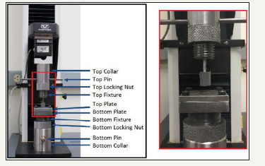
In order to load the samples to fracture using a high precision universal vertical load machine (Instron, model 3345, Norwood, MA), a set of custom fixtures was fabricated to grip the PCB and stainless steel screw of each testing sample. These fixtures, shown in Figure 5, contained a top assembly with a tapped hole at the center of the bottom face to hold the screw securely in place during testing, and a bottom assembly composed of two parallel steel plates, bolted together with a gap twice the height of the PCB substrate thickness. Additionally, the top plate had a center through-hole which allowed the epoxy casting to pass through, while holding the PCB in place.
Figure 5:Upper and lower fixture assemblies with tensile sample.
Results
Each of the three LF solder alloys was tested using the tensile assembly. The results were recorded using the integrated software to the Instron system as the displacement and load to failure of each sample. An example result of this can be seen in Figure 6 where newly exposed faces of both the PCB and bump contain an area corresponding to the fractured IMC.
Figure 6:Newly exposed faces of example fractured sample.
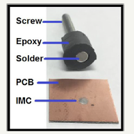
To convert the load values to stresses to allow for comparison to stress values for other solders found in the literature, the areas of the newly exposed fractured surface of the IMC was used, an example of which is shown at the center of the PCB square in Figure 6.
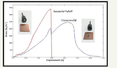
There are two types of plot forms in the results, samples of which are shown in Figure 7. The first is an example of a successful test result (solid curve), while the other is a failure of the epoxy, resulting in an unsuccessful test (dashed curve). The failure occurred due to air pockets within the epoxy forming voids around the interface of the bump and epoxy. These voids weaken the epoxy surrounding the solder to the point that when the load reaches a critical value, these voids decreased the overall strength of the epoxy to the extent that it could not perform its task of remaining adhered to the bump. All unsuccessfully tested samples contained at least one such void, and account for 5 out of the 84 tests conducted for the three solder types, or 5.9% of the total testing group. The remaining 94.1% of the tests concluded in brittle fracture of the IMC
Figure 7:Tensile test result types.
Discussion
At the conclusion of the tensile tests, the median and mean peak stress values for each of the successful tensile tests were analyzed. Box plots of the successful tests for each solder are shown in Figure 8. The raw data for each solder was normally distributed and the mean and median peak values for each solder were calculated within one standard deviation of the mean of each original data set. The median peak pull-off stress values at failure are 13.9MPa, 5.9MPa, and 20.1MPa, for the SnAg, SAC305 and SnCu solders, respectively. The mean pull-off stress values for each solder is shown with a diamond shape within each box, with the standard deviation marked by the vertical whisker lines which terminate at their maximum and minimum values. For each solder, the first and third quartiles of the peak stress results are represented by the portion below the median value and the portion above the median value, respectively, in each box. The first quartile represents the median values of the lower 50% of the data set, and the third quartile represents the median values of the upper 50% of the data set. It is through this graphical representation that one may identify the true behavior of the solders when compared to one another. By using the box plots to examine the median pull-off stress values, it is clear that the two bi-metallic alloys performed with higher mean peak pull-off stress values, and of those two, SnCu is the leading alloy. In addition to the mean and median peak pull-off stress values for the SAC305 solder being lower than the two other solders tests, it also has the largest deviation within the data, while the SnCu solder has both the highest mean and median values and the lowest deviation within the data.
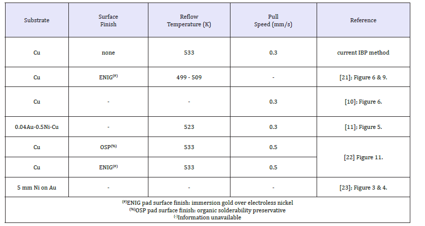
Comparisons of the maximum pull-off stress values for the IBP method were made with those found in the literature. In Figure 9, the solid (red) circles represent the IBP maximum pull-off stress values for each of the LF solders and are compared with maximum pull-off stress values for CBP and HBP methods of the same solder types. The reflow temperatures, pull speeds and surface finishes used for the literature values, when noted in the respective papers, are included in Table 1.
Figure 8:Box plots of pull-off stress values.
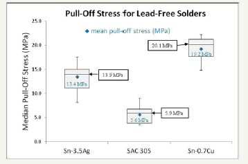
Table 1: Literature comparison information.
The maximum pull-off stresses for the IBP method fall at the low end of the pull-off stress values found in the literature when compared with both the CBP and HBP methods for all three LF solder types. The IBP values are: 18MPa (SnAg), 16MPa (SAC305) and 22MPa (SnCu). The majority of the comparisons found were those for the SnAg solder, which generally had the lowest pull-off stress values of the three solders. In addition for SnAg, all three methods IBP, CBP and HBP, have pull-off stress values on the same order of magnitude, ranging between 15 and 88MPa. The only method found to have a lower pull-off stress than IBP was CBP at 15MPa for the SnAg[11]. Of the comparisons of CBP and HBP for SAC 305 and SnCu, all of the pull-off stress values were an order of magnitude greater than the IBP values. It is suggested that since the copper substrates used in the current IBP work were untreated, that the lower pull-off stress values resulted.
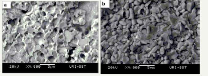
In addition to the tensile tests that were performed on the bump samples, a scanning electron microscope (SEM) (JEOL JSM- 5900LV, JEOL USA Inc, Peabody, MA) was used to perform high magnification of the fracture surfaces to verify that brittle fracture occurred. Examination of the high magnification images in Figure 10, show brittle fracture for the newly exposed faces of the PCB and bump.
Figure 9:Comparison of Maximum Pull-off Stress for IBP method with CBP and HBP methods from literature.

Figure 10:High magnification of SnAg surfaces (a) on PCB face (b) on bump face.
Lastly, in addition to the images of each newly formed surface, the SEM was used to perform Energy Dispersive X-Ray Spectrometry (EDS) to analyze the surface chemistry of both newly exposed faces. Shown in Figure 11a-11d, where Figure 11c corresponds to the boxed location in Figure 11a, and Figure 11d corresponds to the boxed location in Figure 11b, the values of Sn and Ag are nearly identical. Of special note, is that the levels of Cu are also nearly identical for the two positions. This is especially important as the solder in question was SnAg with no Cu present in the mix and this was the first solder tested in the stainless steel crucible, and so no Cu contributed to the solder prior to the formation of the joint. The presence of Cu then shows that material from the substrate was absorbed into the solder and formed the IMC. Additionally, as the same materials are present in roughly the same concentrations on both faces, this shows that the brittle fracture that was identified from the images was through the IMC and not at an interface of the IMC and either the solder or the Cu substrate[21-23].
Conclusion
By combining the positive attributes of both the HBP and CBP direct tensile testing methods, it was possible to develop a novel method for tensile testing the adhesion strength of lead-free solders. The Isotraction Bump Pull (IBP) method and subsequent analyses were able to show the following:
A. That the IBP method conforms to the requirements of the HBP and CBP methods while not adversely impacting the structure of the solder bumps prior to testing;
B. That the results for the IBP method for the Sn-3.5Ag solder falls within the pull-off stress values when compared with CBP and HBP methods in the literature, and is an order of magnitude lower in pull-off stress values when compared with the mechanical behavior of SAC 305 and Sn-0.7 Cu solders using the CBP and HBP methods;
C. That the method identifies the failure mode as that of brittle fracture of the IMC layer.
Acknowledgment
The authors gratefully acknowledge the contributions of Prof. Richard Brown of the Chemical Engineering Department at the University of Rhode Island.
References
- The European parliament and the council of the European union (2003) Directive 2002/95/ec of the European parliament and of the council, UK, pp. 1-18.
- Bieler TR, Hairong J, Lehman L, Kirkpatrick T, Cotts EJ, et al. (2008) Influence of sn grain size and orientation on the thermomechanical response and reliability of pb-free solder joints. Components and Packaging Technologies IEEE Trans 31(2): 370-381.
- Duffy M, Floyd L, Closkey P, Mathuna CO, Tellefsen K, et al. (2001) RF characterisation of no-clean solder flux residues. IMAPS in 2001 International Symposium on Microelectronics, USA, pp. 138-143.
- Glazer J (1994) Microstructure and mechanical properties of pb-free solder alloys for low-cost electronic assembly: a review. Journal of Electronic Materials 23(8): 693-700.
- Moon K, Boettinger WJ, Kattner UR, Biancaniello FS, Handwerker CA (2000) Experimental and thermodynamic assessment of sn-ag-cu solder alloys. Journal of Electronic Materials 29(10): 1122-1136.
- Ochoa F, Williams JJ, Chawla N (2003) Effects of cooling rate on the microstructure and tensile behavior of a sn-3.5 wt.% ag solder. Journal of Electronic Materials 32(12): 1414-1420.
- Chang Y, Hee RR, Young MK, Jin SL, Hae YC, et al. (2009) A new solder wetting layer for pb free solders. Journal of Material Research 24(2): 297-300.
- Darveaux R (2002) Effect of simulation methodology on solder joint crack growth correlation and fatigue life prediction. J Electron Packag 124(3): 147-154.
- Frear DR, Jang JW, Lin JK, Zhang C (2001) Pb-free solders for flip-chip interconnects. JOM 53(6): 28-32.
- Nishikawa H, Komatsu A, Takemoto T (2007) Morphology and pull strength of sn-ag (-co) solder joint with copper pad. Journal of Electronic Materials 36(9): 1137-1143.
- Nishiura M, Nakayama A, Sakatani S, Kohara Y, Uenishi K, et al. (2002) Mechanical strength and microstructure of BGA joints using lead-free solders. Materials Transactions 43(8): 1802-1807.
- Wong EH, Seah SK, van WD, Driel J, Caers N, et al. (2009) Advances in the drop-impact reliability of solder joints for mobile applications. Microelectronics Reliability 49(2): 139-149.
- Gerbracht L, Cox M, Whiting S (2005) Understanding the complexities of solder ball pull testing on BGAs. Advanced Packaging 14(3): 20-21.
- ASTM F459-13 (2013) Standard test methods for measuring pull strength of microelectronic wire bonds. ASTM International, West Conshohocken, USA.
- JEDEC JESD 22-B115, Solder ball pull, JEDEC solid state technology association, Arlington, Virginia.
- Zaal JJ, Hochstenbach HP, Driel WD, Zhang GQ (2009) Solder interconnect reliability under drop impact loading conditions using high-speed cold bump pull. Microelectronics Reliability 49(8): 846-852.
- Cheng SX, Li T, Chandra S (2005) Producing molten metal droplets with a pneumatic droplet-on-demand generator. Journal of Materials Processing Technology 159(3): 295-302.
- Cheng S, Chandra S (2003) A pneumatic droplet-on-demand generator. Experiments in Fluids 34(6): 755-62.
- Chen AU, Basaran OA (2002) A new method for significantly reducing drop radius without reducing nozzle radius in drop-on-demand drop production. Physics of Fluids 14(1): 1-4.
- Amirzadeh A, Raessi M, Chandra S (2013) Producing molten metal droplets smaller than the nozzle diameter using a pneumatic drop-ondemand generator. Experimental Thermal Fluid Science 47(5): 26-33.
- Anselm MK, Roggeman B (2014) Testing inter metallic fragility on enig upon addition of limitless cu. SMT Surface Mount Technology Magazine 29: 30-41.
- Song F, Lee SWR (2006) Investigation of imc thickness effect on the lead-free solder ball attachment strength: comparison between ball shear test and cold bump pull test results. 6th Electronic Components and Technology Conference Proceedings, IEEE, CA, USA, pp. 1196-1203.
- Zingg R, Geelhaar R, Myat C, Struwe A, Krastev E (2015) Comparative tests for lead-free solder bumps. EMPC, Egypt, pp. 1-3.
© 2018 DML Meyer . This is an open access article distributed under the terms of the Creative Commons Attribution License , which permits unrestricted use, distribution, and build upon your work non-commercially.
 a Creative Commons Attribution 4.0 International License. Based on a work at www.crimsonpublishers.com.
Best viewed in


.jpg)


 Editorial Board Registrations
 Submit your Article
 Refer a Friend
 Advertise With Us
.jpg)


.jpg)


.bmp)
.jpg)
.png)
.jpg)


.jpg)


.png)

.png)


.png)


