- Submissions

Full Text
Research & Development in Material Science
Multi-Junction Solar Cells: Snapshots from the First Decade of the Twenty-First Century
Guy Francis Mongelli*
Department of Chemical Engineering, University of Rochester, USA
*Corresponding author: Guy Francis Mongelli, Department of Chemical Engineering, University of Rochester, 500 Wilson Blvd, Rochester, NY, 14627, USA
Submission: February 13, 2018 Published: February 23, 2018
Volume 4 Issue 1 February 2018
Abstract
In this manuscript, the perhaps largest milestones of multi-junction solar cells over the first decade in the twenty-first century will be discussed with particular emphasis on devices with noteworthy commercial and practical viability.
Introduction
Multi-junction solar cells utilize a layered structure of materials to absorb different sections on the solar spectra. These devices are some of the most interesting in emerging alternative energy technologies because they sport the highest efficiencies out of all device structures. Moreover, the efficiencies of these devices are increasing at the greatest rate. They possess high radiation hardness and are most suited for applications in outer space. Optimal engineering includes careful selection of sub cell semiconductor band gaps, the lattice constant of the sub cell crystals, current matching the individual sub-cells, composition of the tunnel layer structure, and minimization of shadowing and resistive affects of the anti-reflection coating. Current structures utilize GalnP, GaAs, and Ge sub-layers with approximate respective band gaps of 1.9eV, 1.4eV, and .6eV. One barrier to their mass production is the costly nature of MBE and MOVPE deposition systems. New materials with more carefully selected band gaps and lattice constants increase charge diffusion lifetimes, decreased dislocation densities and recombination velocities (increased grain sizes), are currently in development. Better control of these properties yields devices with higher efficiencies. The outcomes of tweaking the layers in a MJ cell are not always obvious because charge transport in semiconductors is an emerging field and altering the properties of one layer can appropriate multiple consequences in the overall device performance. Simply utilizing a combinatorial approach to increasing the efficiency would be a futile effort. There too many variables to account for, and a lifetime of random experimentation would not account for the discoveries made through sound application of the governing theories. Therefore careful experimentation is necessary to explore the nature of these devices and to push their efficiencies toward the maximum theoretical limits. Several cases that contributed to our improved understanding of multi-junction solar cells were in the following literature articles.
Discussion
Figure 1:
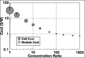
Figure 2: The photo generated current density Jph absorbed in a standard GaAs/GaAs junction and a wide band gap AlGaAs/GalnP tunnel junction.
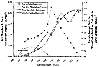
The transition from two-junction to three-junction devices came in the mid-nineties when researchers began adding a low band gap Germanium layer to their two-junction devices. Many articles appeared shortly after NREL and Spectrolab published their work with three junctions (Figure 1). This allowed the cells to absorb light with energy greater than .7eV (wavelength smaller than about 1700nm). The region between .7eV and 1.4eV had been unexplored until then (Figure 2).
Efficiency Increase by King RR [1]
In King's [1] paper, the efficiency of these cells was increased to 30.0% at AM 0, 7.6 suns. The main reason his group cites improved efficiency is better device interfaces (reduced recombination velocity) and crystallinity. The article did not discuss how they quantified the quality of the interfacial structure. However, the figure to the left indicates that they were able to narrow the statistical distribution of crystal lattice constants (unfortunately, no discussion of altered MOVPE technology or conditions) and that this correlated to better devices. Along with these considerations, they simultaneously decreased window resistance while keeping a high blue throughput response, altered the middle layer cell window (which included aluminum doping) and thinned the Ge sub layer to reduce the bulk re-combinations.
The figure to the upper right indicates the improvements in current density from altering the window layer. The new window with aluminum doping decreases absorption throughout the spectra through reducing the band gap wavelength to 675nm from 900nm. This light then can pass through to the Ge layer and be absorbed there. The theoretical current gain integrated from low wavelength to high wavelength is shown.
Here is the IV trace for the record-winning cell at 1 sun. Following is the absorption performance for particular sub cells. This data is taken from making multiple contacts within the device structure and by cutting out windows in parts of the device.
Figure 3: Open-Circuit voltage as a function of full-width half-maximum of X-ray diffraction peaks, for cells grown so that only the middle cell is active.

The strengths of this article lie in its improved efficiency and forward thinking about 4J structure while 3J isn't completely optimized. Quams with the literature arise due to the omission of key details about quantifying interfacial quality and the synthesis methodology that produced more homogeneous crystal structure (Figure 3-5).
Figure 4: Light I-V characteristics for record-efficiency 3J and 2J cells under the AM0 spectrum.
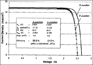
Figure 5: Externa! quantum efficiency of the top, middle and Ge bottom sub cells in the record efficiency 3J cell.
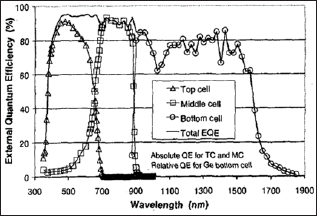
Yamaguchi M [2] Efficiency Enhancement
In Yamaguchi’s [2] article, the efficiency of 3J cells was increased to 33.3% at AM 1.5, 1 sun. This was achieved through increasing the carrier lifetime by optimizing the growth temperature of the added buffer layer. Simultaneously, the surface recombination velocity of the AlInP window (which utilized an advanced double-hetero junction structure) was reduced. The authors say that the double- hetero junction confines holes from passing through the tunnel while increasing carrier diffusion and light penetration.
The figure to the left shows the calculated tunnel peak current density and short-circuit current density Jsc of GaAs bottom cell as a function of band gap energy of tunnel junction. The current of the bottom cell is the critical perameter to by maximize. This requires the incorporation of a large band gap tunnel junction (as close to 2eV as is possible) which has been shown to be difficult to synthesize.
The following figure shows the thoretical limits and experimentally demonstrated efficiencies of different number of sub cell devices. It is important to note that we are not close to tapping these technologies completely yet. More layers would increase these limits further. According to Olsen, 36 layers would provide a theoretical efficiency to 76%; and 86.8% for an infinite number of p-n junctions.
Yamaguchi's [2] article then shows the cost of solar cell devices as a function of concentration and the relative breakdown of the costs between optical components and cell costs. It makes sense that the cost of devices as well as their efficiencies increases as concentration increases. This allows the PV system to generate one watt of power will less cells but more complex optics. There are any implicit and unspecified assumptions here. It is difficult to believe the practicality of this graph. One potential problem is that the cost assumes a lifetime that is uncertain. But assuming that it is true, is still does not estimate when we’ll be able to make optics that can achieve concentration ratios of 1000. Still, it is useful for PV researchers to show this because it gives cause for investment in both PV and optics research.
Yamaguchi cites that moving forward, researchers need to reduce dislocation densities to below 5*10-5 per cm2 and increase the grain size to greater than .05cm. The strengths of this article include its certified increase in efficiency and the incorporation of the synthesized cells into several satellite designs. This is an asset because it shows corporate interest in these technologies (Figure 6 & 7).
Figure 6:
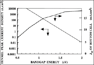
Figure 7:
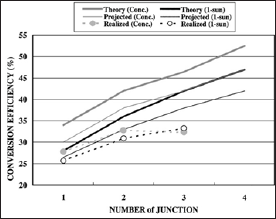
King RR [3] Enhances Again
The major claim of this work, independently verified by NREL, is that the efficiency of a 3J cell of 40.7% was achieved at 240 suns. This increase was attributed to better current matching of the subcells and a better AR coating/grid design to minimize shadowing. The authors consider several device structures, including two 3J structures and a 4J structure. The difference between the 3J structures is whether or not the layers were forced to be lattice matched or not. Lattice matching altered the structure of the middle layer, constraining the band gap to a certain value. The metamorphic crystals allowed for a variety of band gaps to be tested but there were some dislocations introduced into the crystal.
Figure 8:
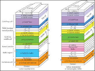
Figure 9:

The reason that the metamorphic devices have higher efficiencies is shown in the current density trace. Without forcing the lattice constant to a particular value, a narrower band gap can be achieved through indium doping in the middle layer. Since the middle layer was current limiting the system, this took current from the bottom layer and introduced it into the middle layer. The overall device current is the minimum of the individual currents, so altering the middle layer band gap improved the performance of the device enough to break 40%.
King's [3] paper includes some work on 4J device structures. The difference between a 3J and 4J cell is that the 4J cell contains an extra, aluminum-doped GaAs sub cell. The addition of aluminum shifts the band gap to 1.6eV. This allows for some energy to be picked up that is missed by the GalnP cell due to its low quantum efficiency at that energy level (Figure 8). The device efficiency is 35.7%. This is a great efficiency since it beats out most other solar cell technologies. Currently, 3J cells are more efficient. This article is the most complete out of the three. It includes a plethora of theoretical and experimental work, boasting higher cell efficiencies in multiple technologies (Figure 9).
Yang et al. [4] Enhancement
This is an interesting article about the inclusion of gold nanoparticles into solar cell structures can utilize plasmon resonances to absorb light and improve device efficiencies. However, it must be noted that this enhancement may have come partially from the increase in the internal quantum efficiency, either solely but, perhaps, also combinedly, and perhaps more significantly, from the increase of the in-coupling efficiency from the use of the nanoparticles on the device surface. The in-coupling efficiency being the analogous to the out-coupling efficiency in the LEDs and OLEDs. Further studies might seek out to quantify and express the relative contributions of these effects to the net enhancement.
Conclusion
These articles discussed showcase King [1] and Yamaguchi's [2] developments in the field of solar cell research. Both authors have made advancements in multi-junction devices that assisted in bringing efficiencies above 40%. Observation of their work has given insight into the three critical parameters that are being experimented with in multi-junction devices: current matching, sub cell band gap tuning and layer thickness. Commercial and governmental application in space requires the acquisition of higher efficiency multi-junction solar cell technologies; their high radiation hardness making them the obvious choice. To achieve this it is imperative and scientists and engineers get better at tuning the band gaps of semiconductors through doping of sub layers and alteration of lattice constants, increase the number of sub cell layers to increase energy absorption throughout the entire solar spectra, continue tweaking tunnel junction characteristics to increase electron throughput and decrease their resistivities, and to develop MBE/MOCVD technologies that are cheaper to operate.
Acknowledgement
We are very grateful to Professor Ahmed Labidi for his fruitful advices and stimulating discussions.
References
- King RR (2000) Next-generation, high-efficiency Ill-V multi-junction solar cells. 28th Photovoltaic Specialists Conference, Anchorage, AK, USA, p. 998.
- Yamaguchi M (2003) III-V compound multi-junction solar cells: present and future. Solar Energy Materials & Solar Cells 75(1-2): 261-269.
- King RR (2007) Advances in high-efficiency III-V multi-junction solar cell. Advances in Optoelectronics, Article ID 29523: 8.
- Yang MD, Liu YK, Shen JL, Wu CH, Lin CA, et al. (2008) Improvement of conversion efficiency for MJ solar cells by incorporation of Au nanoclusters. Optics Express 16(20): 15754.
© 2018 Guy Francis Mongelli. This is an open access article distributed under the terms of the Creative Commons Attribution License , which permits unrestricted use, distribution, and build upon your work non-commercially.
 a Creative Commons Attribution 4.0 International License. Based on a work at www.crimsonpublishers.com.
Best viewed in


.jpg)


 Editorial Board Registrations
 Submit your Article
 Refer a Friend
 Advertise With Us
.jpg)


.jpg)


.bmp)
.jpg)
.png)
.jpg)


.jpg)


.png)

.png)


.png)


