
- About Us
- Information
-

The Author ensures that the research has been conducted responsibly and ethically with adherence to all relevant regulations. read more..
- For Authors
- For Reviewer
- Manuscript Guidelines
- Membership
- Publication Ethics
-
- Journals
- Reprints
- e-Books
- Videos
- Policies
- Contact Us
 COVID-19
- Submissions


Full Text
Research & Development in Material Science
A Nano Capacitor Including Graphene Layers Composed with Doped Boron and Nitrogen
Seyedehmarzieh Sadatchoobeh1, Karim Zare1 and Majid Monajjemi2*
1Department of Chemistry, Islamic Azad University, Iran
2Department of Chemical Engineering, Islamic Azad University, Iran
*Corresponding author: Majid Monajjemi, Department of Chemical Engineering, Central Tehran Branch, Islamic Azad University, Tehran, Iran
Submission: December 18, 2017; Published: February 23, 2018

ISSN: 2576-8840Volume3 Issue5
Abstract
In this study, it has been found a configuration including dopant atoms which are replaced in a diagonal line through hand-running atoms from each other. Those are more favorable energetically, and the configuration with atoms of boron and nitrogen are more stable with binding energies. This phenomenon confirms the homogeneous B-substitution that may be easier than the other atoms such as N-substitution. The root of these differences might be affected the structure of B-C bonds which are about 0.5% longer than the C-C bond. Band-gap is opened through the effect of substitution B atom doping on the structure of graphene and the Fermi levels lies in the valence and conduction bands. It has been shown a model of a nanoscale dielectric capacitor composed of a few dopants including metallic graphene layers separated by an insulating medium containing a few h-BN layers
Keywords: Nano capacitor; Graphene; Doping; Boron nitride sheet
Introduction
Graphene individually has a structural flexibility due to its electronic properties. Because of electronic flexibilities, graphene might be fitted chemically in a deposit metal atoms on top [1], The deposit molecules on it [2], incorporated nitrogen and boron in their structures [3] and doped atoms inside the sheets. They can be used in a field of the electronics, capacitors, superconductors, in batteries and diodes. The considerable tends of graphene are the Dirac solid, with the electron energies being linearly dependent on the wave vectors near the vertices of the hexagonal Brillouin zones [4] . Complete histories for the rising of graphene have given by Geim & Novoselov [5].
In this work the properties of various dopants with the electronic structures of a few-layer graphene into two side electrodes in the capacitor has been studied. In this matter, it has been investigated a nano-capacitor through B- and N-doped graphene bilayers employing different strategy for its structure and properties. The B and N atoms are the natural templates for doping in graphene due to their similar atomic size as that of C and of their hole acceptors and electron donors characters for substitution Band N-doping, respectively.
It has been modeled by two configurations of doped bi-layer graphene including various atoms such as (h-BN)n sheets (n=1- 4). Our nanoscale capacitors model are composed of hexagonal (h-BN)n layers (n=1- 4), which are stacked between two graphene electrodes. The single and multi-layers of (h-BN)n are wide band gap insulators, so they can be applied as a dielectric material between metallic graphene layers. An effort has been accomplished for understanding the theoretical basis for the nanoscale dielectric capacitors which are professional to another system of energy storage. In fact, capacitor at nanoscale has been developed as one of the most expecting energies storages mediums [6,7].
That h-BN layers of each thickness might be grown on the graphene electrodes it has been already shown both experimentally [8] and theoretically [9,10]. It is also perpendicular carbon to grow BN chains (also available) on top of the graphene and h-BN single layers [11,12].
At the nanoscales, since the separation thickness of capacitors model can be as smaller as a nanometer size, the stored energy has to be calculated from the first principle calculation [12-14] which allows to treat the distribution of only one kind of excess positive or negative charges at a time (in the same system) [13-16]. In this work it has found a significant increasing of capacitance and negative quantum capacitance based on percentages of B dopants and thickness of h-BN layers.
Via applying an external electric fields perpendicular to the graphene electrodes the charge separation might be achieved in this situation and simulates of the operation by the surface charge with opposite sign initially stored on different doped plates create perpendicular electric fields. The shorting of these two plates and hence the discharges of the capacitors are prevented by placing sufficient quantities of h-BN layers between doped graphene plates.
Based on electrostatic theory the geometric capacitance densities, "cg", is related to the applied Voltage,ΔVapp as the equation  where σ is the surface charge densities, εr, ε0 are the dielectric constant and absolute permittivities respectively. Ajayan [17] has found a significant increasing in the capacitance below the thickness of "5nm", more than what is predicted by classical electrostatic. This unusual increase in a capacitance is because of the negative quantum capacitance that this particular materials system exhibits (Figure 1).
Figure 1: Nano-capacitors models.

Theoretical Back Grounds and Model
Figure 2: Density versus atomic position.

The patterns of negative quantum effects in the interaction between the gold electrodes and h-BN films have investigated by Ajayan [17]. Ajayan have determined the dielectric permittivities as a function of dielectric size through ab-inito calculation using the SIESTA atomistic simulation package [17].The Nano-dielectric- capacitor models or NDC have been successfully used for simulating stacking structure of G/h-BN/G [18]. Density functional theory with the van der Waals density functional for modeling the exchange- correlation energy of Au and h-BN have been employed through a relativistic pseudo-potential method [19-21] (Figure 2).
It has been considered two isolated metal-doped-graphene (MDG) layers where each one is fully charged by Q electrons per primitive unit-cells . The NDC models with (h-BN)n layers (n=1, 2, 3) as dielectric are covered through two parallel MDG (M=Mg, Al, Si, B) layers. In our model the interlayer distances for h-BN varies in the range of {3.0-5.0} A, which they are the beset interaction, while the 3.55 is in a reasonable data and agreement with the experimental variables (3.306 A) [22] and also theoretical values [23] (Figure 3).
Figure 3: LOL color field map.

Recently a few works [7,16,22-25] indicate an abnormal increasing in the capacitance along decreasing size of nano-system including negative quantum capacitance. These effects arise from many-body interaction because the chemical potentials of the electron decrease with increasing of electron density. Maccuci [26,27] exhibited a capacitance of quantum dots. Another work on non-linear quantum capacitances [28] and atomic junctions [29] has been investigated by Wang et al. The hybrid capacitances and
then quantum capacitances are related to the net capacitances, C,
with the relation  and the values of CQ are many orders of magnitude greater than the Cg, and hence its effect usually appears only in the very small systems [17].
The QM components are development of the density of state (DoS) for the metal electrodes, and their Thomas-Fermi screening length. Hence the hybrid capacitances of each nano-capacitors architecture are given as: Where C_t is the total
capacitance of the nano-capacitors, in addition Cg is the classical capacitances, CQ1 and CQ2 are the quantum capacitance due to their finite DoS of the metal doped graphene electrodes (M1G, and M2G, respectively).
Where C_t is the total
capacitance of the nano-capacitors, in addition Cg is the classical capacitances, CQ1 and CQ2 are the quantum capacitance due to their finite DoS of the metal doped graphene electrodes (M1G, and M2G, respectively).

 [30,31] of either electrodes.
  which for metal for metal=Au [31]. Hence the hybrid capacitances due to its composition of both classical and quantum capacitances can be
Computational Details
Calculations were performed by GAMESS-US package [32]. In this work, we have focused on getting the results from DFT methods for the non-bonded interaction of graphene sheets composed with boron and nitrogen doping. They also are monotonous through the comparison between different situations. Density functional theory with the van der Waals density functional (vdW-DF) has been applied to model the exchange-correlation energy of doped graphene and h-BN [19]. The double Z-basis sets with polarization orbital (DZP) was used for doping while single Z-basis sets including polarization orbitals (SZP) was employed for the h-BN layers, respectively. The m062x, m06-L, and m06-HF are new method within good correspondence in the non-bonded calculation and are suitable for the energy of the distances between two fragments in the capacitors. For a non-covalent interaction; B3LYP is unable for describing van der Waals [33,34] capacitor systems in mediumrange interactions, such as the interactions of two electrode and dielectric sheets.
In addition, some recent study has shown the inaccuracy of the medium-range exchange energies leads to large systematic error in the prediction of molecular properties [35-39]. Graphene is known in 2-D honeycomb structures and the B and N doped graphene will be assumed to have a similar structure, unless violated by energies minimization considerations. A monolayer of G was optimized and allowed for relax to its minimum energies structure; it contains 76 atoms with zigzag edges. The edges were saturated with the hydrogen atoms to neutralize the valance of terminal carbons, reducing edges effects [40].
Geometry optimizations and electronic structure calculation have been performed using the m06 (DFT) which the approaches are based on an iterative solution of the Kohn-Sham equation [41] of the density function theory in a plane-wave set with the projector-augmented wave pseudo-potentials. The Perdew-Burke- Ernzerhof (PBE) [42] exchange-correlation (XC) functional of the generalized gradient approximation (GGA) is adopted. The optimizations of the lattice constants and the atomic coordinates are made by the minimization of the total energies. The dimension of capacitors has been set as 12.388x3. 95x8.52 Å (scheme 1) and the sheets are separated by various distance (Table 1 & 2) along the perpendicular direction to avoid interlayer interaction. During all of the calculations processes, except for the band determination, the partial occupancy was treated using the tetrahedron methodology with Blochl [43] corrections.
In our model the electrodes have doped through various percentage of boron atoms which are likely to adjust for surrounding C atoms of the host. Therefore when the graphene sheet is doped with one boron atoms, the boron atoms also undergoes sp2 hybridization and due to the nearly same size of C and B, no significant distortion in 2-D structure of graphene are expected, except for change in adjoining bond lengths. By doping boron atoms in graphene Fermi level shifts significantly below the Dirac point resulting into a p-type doping and the symmetries of graphene have broken in two graphene sub-lattices because of introduction of B atom and causes for changing the behavior of graphene from semimetal to conductors. The charges transfer and electrostatic potential-derived charges were also calculated using the Besler [43], Chirlian [44], Brneman [45] (Figure 4).
Figure 4: Contour map of ELF.

Figure 5: Average local ionization energy.

The charges calculation method based on molecular electrostatic potentials (MESP) fitting are not well-suited for treating larger system where some of the innermost atoms are located far away from the points at which the MESP is computed. In such a condition, variation of the innermost atomic charge will not lead to significant changing of the MESP outside of the molecule, meaning that the accurate value for the innermost atomic charge are not well-determined by MESP outside of the molecules. The representative atomic charges for molecule should be computed as the average value over several molecular conformations. A detailed overview of the effect of the basis set and the Hamiltonian on the charge distribution can be found in [46,47]. We have also extracted the charges density profiles from the first-principles calculation through an averaging process described [48,49].
Although infinite graphene sheet are intrinsically metallic, our BG system exhibits an increasing in the metallic properties. The interaction energies for capacitor were calculated in all items as the equation: + ΔES(eV) = {Ec -(2ECopant-G + Eh-BN)}+EBSSE (9) where the "ΔEs " is the stability energy of capacitor. The fundamental of this work is based on our previous works [50-84].
Results and Discussion
In this work, the values of the distance between graphene layers capping h-BN layers, dielectric constants of the layered h-BN sheets (k), magnitude of the charge on the graphene electrode, the stabilities energies of capacitors (in eV) and potential difference between the electrodes of graphene plates are listed in Tables 1-3. Using various percentages dopants in tables indicate proper situations for boron and nitrogen dopants in graphene electrodes.
Although the dielectric strength can be deduced from the band structure of BN spacer, here we have calculated the dielectric constant straightly from (eq.1), which is much more accurate than the other methods. The potential energy difference between the two graphene layers,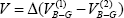 are shown in Table 3. In addition, according to electronic structures we have considered two isolated graphene layers, which each one is doped by boron atoms in various distances. They have been charged by q+m-G and q-m-G electrons per primitive unit-cells
 which are shown in Tables 1-3.
The atomic structures, interlayer spacing, relative positions of the layers and the cell parameters are optimized. It is obvious that for BN spacer consisting of a few layers, the different voltages among electrodes depend on various conditions such as nonequilibrium state, the coupling between graphene and adjacent h-BN, etc. and require a thorough analysis. In Tables 1-3, we have shown comparison among the stability and Gap Energy (eV) of various dopants' percentage.
Conclusion
In this study, we have shown the model of a nanoscale dielectric capacitor composed of various percentage dopants including h-BN and graphene sheets separated by an insulating medium containing a few layers. We showed that in this model, the percentage dopants play significant roles in the nano capacitors. The capacitor with medium percentage of boron nitrides dopants has the high dielectric constant. Our theoretical results show that the relative permittivity of dielectric can be higher than that of no percentage of boron nitride.
References
- Ostinga JB, Heersche HB, Liu X, Morpuzo A, Vanderspyen LMK (2008)Gate-induced insulating state in bilayer graphene devices. Nature Mater 7: 151-157.
- Dressalhaus MS, Dresselhaus G, Eklunch PC (1995) Science of fullerenes and carbon nanotubes, (1st edn), Academic Press,San Diego,CA,p.760.
- Tanuma S, Kanimura H (1985) Progress of research in Japan (World Scientific, Singapore).
- Castro AHN, Guinea F, Peres NMR, Novoselov KS, Geim AK (2009) The electronic properties of graphene. Rev Mod Phys 81(1): 109.
- Geim AK, Novoselov KS (2007) The rise of Graphene. Nat Mat 6(3): 183191.
- Yildirim T, Ciraci S (2005) Titanium-decorated carbon nanotubes as a potential high-capacity hydrogen storage medium. Titanium Phys Rev Lett 94: 175501.
- Durgun E, Ciraci S, Zhou W, Yildirim T (2006) Transition-metal-ethylene complexes as high-capacity hydrogen-storage media. T Phys Rev Lett 97: 226102.
- Liu Z, Song L, Zhao S, Huang J, Ma L, et al. (2011) Direct growth of graphene/hexagonal boron nitride stacked layers. M Nano Lett 11(5): 2032-2037.
- Özişelik VO, Cahangirov S, Ciraci S (2012) Epitaxial growth mechanisms of graphene and effects of substrates. Epitaxial Phys Rev B 85: 235456.
- Sachs B, Wehling TO, Katsnelson MI Lichtenstein AI (2011) Adhesion and electronic structure of graphene on hexagonal boron nitride substrates. Phys Rev B 84: 195414.
- Özşelik VO, Ciraci S (2012) Self-assembly mechanisms of short atomic chains on single-layer graphene and boron nitride. Phys Rev B 86: 155421.
- Ataca C, Ciraci S (2011) Perpendicular growth of carbon chains on graphene from first-principles. Phys Rev B 83: 235417.
- Chan KT, Lee H, Cohen ML (2011) Gated adatoms on graphene studied with first-principles calculations. Phys Rev B 83: 035405.
- Chan KT, Lee H, Cohen ML (2011) Possibility of transforming the electronic structure of one species of graphene adatoms into that of another by application of gate voltage: First-principles calculations. Phys Rev B 84: 165419.
- Suarez AM, Radovic LR, Bar-Ziv E, Sofo JO (2011) Gate-voltage control of oxygen diffusion on graphene. Phys Rev Lett 106: 146802.
- Topsakal M, Ciraci S (2012) Effects of static charging and exfoliation of layered crystals. Phys Rev B 85: 045121.
- Gang S, Yuranan H, Liu Z, Gong Y, Gao W, et al. (2014) Boron nitride- graphene nanocapacitor and the origins of anomalous size-dependent increase of capacitance. Nano Lett 14(4): 1739-1744.
- Ozcelik VO, Ciraci SJ (2013) Size dependence in the stabilities and electronic properties of a-graphyne and its boron nitride analogue. Phys Chem C 117(29): 15327-15334.
- Dion M, Rydberg H, Schroder E, Langreth DC, Lundqvist BI (2004) Collisionally induced transport in periodic potentials. Phys Rev Lett 92: 24640.
- Fernandez EM, Soler JM, Garzon IL, Balbas LC (2004) Trends in the structure and bonding of noble metal clusters. Phys Rev B 70(16): 165403-165414.
- Gao M, Lyalin A, Taketsugu (2012) Catalytic Activity of Au and Au2 on the h-BN Surface: Adsorption and Activation of O2. J Phys Chem 116: 9054.
- Paszkowicz W, Pelka JB, Knapp M, Szyszko T, Podsiadlo S (2002) Lattice parameters and anisotropic thermal expansion of hexagonal boron nitride in the 10-297.5 K temperature range. Appl Phys A 75(3): 431435.
- Hamada I, Otani M (2010) Comparative van der Waals density- functional study of graphene on metal surfaces. Phys Rev B 82: 153412.
- Liu Z, Zhan YJ, Shi G, Moldovan S, Gharbi M (2012) Nat Commun 3: 879.
- Liu Z, Ma LL, Shi G, Zhou W, Gong YJ, et al. (2013) Nat Nanotechnol 8(2): 119-124.
- Macucci M (1997) Differential capacitance between circular stacked quantum dots. Physica E 1(1-4): 7-14.
- Macucci M, Hess K, Iafrate GJ (1993) Electronic energy spectrum and the concept of capacitance in quantum dots. Phys Rev B 48: 17354-17363.
- Wang B, Zhao X, Wang J, Guo H (1999) Appl Phys Lett 74: 2887-2889.
- Wang J, Guo H, Mozos JL, Wan CC, Taraschi G, et al. (1998) Capacitance of atomic junctions . Phys Rev Lett 80(19): 4277-4280.
- Mulak J (1996) The thomas-fermi type screening of the crystal field multipole moments. Journal of Solid State Chemistry 124(1): 182-189.
- Ashcroft NW, Mermin ND (1976) Solid state physics: Saunders College Publishing, USA.
- Schmidt MW, Baldridge KK, Boatz, Elbert ST, Gordon MS, et al. (2004) General atomic and molecular electronic structure system. J Compt chem 14(11): 1347-1363.
- Zhao Y, Donald G, Truhlar (2008) The M06 suite of density functionals for main group thermochemistry, thermochemical kinetics, noncovalent interactions, excited states, and transition elements: two new functionals and systematic testing of four M06-class functionals and 12 other functional. Theor Chem Account 120(1-3): 215-241
- Zhao Y, Donald G. Truhlar (2008) Density functionals with broad applicability in chemistry. Accounts of Chemical Research 41(2): 157167.
- Check CE, Gilbert TM (2005) Progressive systematic underestimation of reaction energies by the B3LYP model as the number of C-C bonds increases: why organic chemists should use multiple DFT models for calculations involving polycarbon hydrocarbons. J Org Chem 70(24): 9828-9834.
- Grimme S, Seemingly (2006) Seemingly simple stereoelectronic effects in alkane isomers and the implications for kohn-sham density functional theory. Angew Chem Int 45(27): 4460-4464.
- Wodrich MD, Corminboeuf C, Schleyer (2006) Systematic errors in computed alkane energies using B3LYP and other popular dft functionals. P R Org Lett 8(17): 3631-3634.
- Schreiner PR Fokin AA Pascal RA, de Meijere A (2006) Many density functional theory approaches fail to give reliable large hydrocarbon isomer energy differences. Org Lett 8(17): 3635-3638.
- Zhao Y, Truhlar DG (2006) A density functional that accounts for medium-range correlation energies in organic chemistry. Org Lett 8(25): 5753-5755.
- Ao Z ,Yang J ,Li S, Jiang Q (2008) Enhancement of CO detection in Al doped graphene. Chem Phys Lett 461(4-6): 276-279.
- Kohn W, Sham LJ (1965) Self-consistent equations including exchange and correlation effects. Phys Rev 140: 1133-1138.
- Perdew JP, Burke K, (1996) Generalized gradient approximation made simple. Ernzerh of Phys Rev Lett 77: 3865-3868.
- Blöchl PE, Jepsend O, Andersen OK (1994) Improved tetrahedron method for Brillouin-zone integrations. Phys Rev B 49: 16223.
- Besler BH, Merz KM, Kollman PA (1990) Atomic charges derived from semiempirical methods. J comp Chem 11(4): 431-439.
- Chirlian LE, Francl MM (1987) Atomic charges derived from electrostatic potentials: A detailed study. J comp chem 8(6): 894.
- Brneman CM, Wiberg KB (1990) Determining atom-centered monopoles from molecular electrostatic potentials. The need for high sampling density in formamide conformational analysis. J Comp Chem 11(3): 361-373.
- Martin F, Zipse H (2005) Charge distribution in the water molecule-A comparison of methods. J Comp Chem 26(1): 97-105.
- Balderchi A, Baroni S, Resta R (1988) Evolution of the dendritic instability in solidifying succinonitrile. Phys Rev Lett 61: 173.
- Monajjemi M, Bagheri S, Moosavi MS, Moradiyeh N, Zakeri M, et al. (2015) Symmetry Breaking of B2N(-,0,t): An Aspect of the Electric Poten-tial and Atomic Charges. Molecules 20: 21636-21657.
- Monajjemi M, Mahdavian L, Mollaamin F (2008) Characterization of nanocrystalline silicon germanium film and nanotube in adsorption gas by Monte Carlo and Langevin dynamic simulation . Bull Chem Soc Ethiop 22(2): 277-286.
- Monajjemi M, Farahani N, Mollaamin F (2012) Thermodynamic study of solvent effects on nanostructures: phosphatidylserine and phospha- tidylinositol membranes. Physics and Chemistry of Liquids 50(2): 161172.
- Sarasia EM, Afsharnezhad S, Honarparvar B, Mollaamin F, Monajjemi M (2011) Theoretical study of solvent effect on NMR shielding tensors of luciferin derivatives . Phys Chem Liq 49(5): 561-571
- Monajjemi M, Lee VS, Khaleghian M, Honarparvar B, Mollaamin F (2010) Theoretical Description of Electromagnetic Nonbonded Interactions of Radical, Cationic, and Anionic NH2BHNBHNH2 Inside of the B18N18 Nanoring. J Phys Chem C 114: 15315.
- Monajjemi M (2012) Quantum investigation of non-bonded interaction between the B15N15 ring and BH2NBH2 (radical, cation, anion) systems: a nano molecularmotor. Struct Chem 23: 551-580.
- Monajjemi M, Boggs JE (2013) A New Generation of BnNn Rings as a Supplement to Boron Nitride Tubes and Cages. J Phys Chem 117: 1670-1684.
- Monajjemi M, Chegini H, Mollaamin F, Farahani P (2011) Theoretical studies of solvent effect on normal mode analysis and thermodynamic properties of zigzag (5,0) carbon nanotube. Fullerenes, Nanotubes, and Carbon Nanostructures 19(5): 469-482.
- Monajjemi M, Khaleghian M (2011) EPR Study of Electronic Structure of [CoF6]3-and B18N18 Nano Ring Field Effects on Octahedral Complex. Journal of Cluster Science 22(4): 673-692.
- Monajjemi M (2013) Non bonded interaction between BnNn (stator) and BN(-,0,t) B(rotor) systems: A quantum rotation in IR region. Chemical Physics 425: 29-45.
- Mollaamin F, Monajjemi M (2012) Fractal dimension on carbon nano- tube-polymer composite materials using percolation theory. Journal of Computational and Theoretical Nanoscience 9(4): 597-601.
- Monajjemi M, Hosseini MS, Mollaamin F (2013) Theoretical Study of Boron Nitride Nanotubes with Armchair Forms. Fullerenes, Nanotubes, and Carbon Nanostructures 21(5): 381-393.
- Monajjemi M, Rajaeian E, Mollaamin F, Naderi F, Saki S (2008) Investigation of NMR shielding tensors in 1,3 dipolar cycloadditions: solvents dielectric effect. Physics and Chemistry of Liquids. 46(3): 299-306.
- Fazaeli R, Monajjemi M, Ataherian F, Zare K (2002) Solvent effects on relative stabilities and 14N NMR shielding of cytosine tautomers: continuous set of gauge transformation calculation using polarizable continuum model. Journal of Molecular Structure: THEOCHEM 581(1-3): 51-58.
- Monajjemi M, Wayne, Robert, Boggs JE (2014) NMR contour maps as a new parameter of carboxyl's OH groups in amino acids recognition: A reason of tRNA-amino acid conjugation. Chemical Physics 433: 1-11.
- Monajjemi M, Afsharnezhad S, Jaafari MR, Abdolahi T, Nikosade A(2007) NMR shielding and a thermodynamic study of the effect of environmental exposure to petrochemical solvent on DPPC, an important component of lung surfactant. Russian J physi chem 81(12): 1956-1963.
- Nafisi S, Monajemi M, Ebrahimi S (2004) The effects of mono- and divalent metal cations on the solution structure of caffeine and theophylline. Journal of Molecular Structure 705(1-3): 35-39.
- Monajjemi M, Razavian MH, Mollaamin F, Naderi F, Honarparvar B (2008) A theoretical thermochemical study of solute-solvent dielectric effects in the displacement of codon-anticodon base pairs. Russian J Physi Chem 82(13): 2277-2285.
- Monajjemi M, Falahati M, Mollaamin F (2013) Computational investigation on alcohol nanosensors in combination with carbon nanotube: a Monte Carlo and ab initio simulation. Ionics 19(1): 155-164.
- Monajjemi M,, Chahkandi B (2005) Theoretical investigation of hydrogen bonding in Watson-Crick, Hoogestein and their reversed and other models: comparison and analysis for configurations of adenine-thy- mine base pairs in 9 models. Journal of Molecular Structure: THEO- CHEM 714(1): 43-60.
- Monajjemi M, Baheri H, Mollaamin F (2011) A percolation model for carbon nanotube-polymer composites using the Mandelbrot-Given curve. Journal of Structural Chemistry 52(1): 54-59.
- Monajjemi M, Heshmat M, Haeri HH (2006) QM/MM model study on properties and structure of some antibiotics in gas phase: Comparison of energy and NMR chemical shift. Biochemistry (Moscow) 71(1): S113-S122.
- Monajjemi M, Mollaamin F (2012) Molecular modeling study of drug- dna combined to single walled carbon nanotube. Journal of Cluster Science 23(2): 259-272.
- Monajjemi M, Khaleghian M, Mollaamin F (2010) Theoretical study of the intermolecular potential energy and second virial coefficient in the mixtures of CH4 and Kr gases: a comparison with experimental data. Molecular Simulation 36(11): 865-870.
- Monajjemi M, Chahkandi B, Zare K, Amiri A (2005) Study of the hydrogen bond in different orientations of adenine-thymine base pairs: An ab initio study. Biochemistry (Mosc) 70(3): 366-376.
- Mollaamin F, Monajjemi M (2012) DFT outlook of solvent effect on function of nano bioorganic drugs. Physics and Chemistry of Liquids 50(5): 596-604.
- Lee VS, Nimmanpipug P, Mollaamin F, Kungwan N, Thanasanvorakun et al. (2009) Investigation of single wall carbon nanotubes electrical properties and normal mode analysis: Dielectric effects. Russian J Physi Chem 83(13): 2288-2296.
- Jalilian H, Monajjemi M (2015) Capacitor simulation including of X-doped graphene (X = Li, Be, B) as two electrodes and (h-BN)m (m = 1-4) as the insulator . Japanese Journal of Applied Physics 54(8): 085101.
- Monajjemi M, Naderi F, Mollaamin F, Khaleghian M (2012) Drug design outlook by calculation of second virial coefficient as a nano study. J Mex Chem Soc 56(2): 207-211.
- Monajjemi M, Mollaamin F, Gholami MR, Yoozbashizadeh H, Sadr- nezhaad SK, et al. (2003) Quantum chemical parameters of some organic corrosion inhibitors, pyridine, 2-picoline 4-picoline and 2,4-luti- dine, adsorption at aluminum surface in hydrocholoric and nitric acids and comparison between two acidic media. MGMC 26(6): 349-361.
- Monajjemi M, Khosravi M, Honarparvar B, Mollaamin F (2011) Substituent and solvent effects on the structural bioactivity and anticancer characteristic of catechin as a bioactive constituent of green tea. Int J Quant Chem 111; 2771-2777.
- Ghiasi R, Monajjemi M (2007) Theoretical study of borthiin and its derivatives: structure and aromaticity. Journal of Sulfur Chemistry 28(5): 505-511.
- Monajjemi M, Kharghanian L, Khaleghian M, Chegini H (2014) Quantum study of amino acid bind to carbon nanotube in view of magnetic properties. Fullerenes Nanotubes and Carbon Nanostructures 22(8): 709-725.
- Mahdavian L, Monajjemi M (2010) Alcohol sensors based on SWNT as chemical sensors: Monte Carlo and Langevin dynamics simulation. Microelectronics Journal 41(2-3): 142-149.
- Amiri A, Monajjemi M, Ketabi S (2007) Quantum simulation on donor and acceptor II calix [4]arene substrate and alkali metal ions: the driven inclusion. Physics and Chemistry of Liquids 45(4): 425-433.
- Amiri A, Monajjemi M, Zare K, Ketabi S (2006) Complexation behaviour of p-t -butyl-calix[ 4]arene propoxy derivatives toward alkali metal cations in chloroform. Physics and Chemistry of Liquids 44(4): 449-456.
© 2018 Seyedehmarzieh Sadatchoobeh, et al. This is an open access article distributed under the terms of the Creative Commons Attribution License , which permits unrestricted use, distribution, and build upon your work non-commercially.
Editor In Chief


.jpg)


Signup for Newsletter

Quick Links
 Editorial Board Registrations
 Submit your Article
 Refer a Friend
 Advertise With Us
Our Recent Edition

.jpg)


Top Editors


.jpg)


.bmp)
.jpg)
.png)
.jpg)


.jpg)


.png)

.png)


.png)


Financial Support

Sponsors

Latest e-Books

Latest Video

 a Creative Commons Attribution 4.0 International License. Based on a work at www.crimsonpublishers.com.
Best viewed in
a Creative Commons Attribution 4.0 International License. Based on a work at www.crimsonpublishers.com.
Best viewed in