- Submissions

Full Text
Peer Review Journal of Solar & Photoenergy Systems
Enhancement of Spectral Response and Quantum Efficiency of Silicon-Based Devices Coated with Copper Oxide Nanoparticles
Oday A Hammadi*
Department of Physics, Iraq
*Corresponding author: Enhancement of Spectral Response and Quantum Efficiency of Silicon-Based Devices Coated with Copper Oxide Nanoparticles
Submission: September 16, 2021;Published: January 31, 2022

Volume2 Issue1 January, 2022
Abstract
In this work, the spectral response and quantum efficiency of silicon-based photonic device were enhanced by coating the top surface of silicon with copper oxide nanoparticles. This enhancement is based on the deposition of 10-15nm nanoparticles on silicon surface of high roughness (~110nm) to fill the volume between surface spikes. The spectral response was increased by 37% in the wavelength range of 720-880nm while the quantum efficiency was increased by 18% as the wavelength corresponding to the maximum efficiency was shifted from 580 to 680nm.
Keywords: Silicon devices; Nanoparticles; Photodetectors; Surface roughness
Introduction
Silicon devices still the main components of modern photonics and optoelectronics despite the drastic developments in new semiconductors and their devices. This may continue for decades as the silicon and its devices are reasonably cheaper, easier to fabricate, and much more reliable [1-4]. Consequently, the integration between silicon devices in the photonic and optoelectronic systems and networks can reach ultra-high levels [5-7].
The performance of silicon photodetectors was found highly dependent of the surface roughness of silicon substrate [8-10]. As the surface roughness is increased, the absorption of incident radiation is increased too. Hence, the conversion efficiency of silicon device is accordingly increased [11-13]. Plasma etching of a silicon substrate can be effectively used to form homogeneous and highly rough surfaces at low cost and high reproducibility [14,15]. Nanoparticles can be successfully used to compensate the surface roughness as they can fill the spaces between spikes of such surface [16]. For high levels of roughness, the effect of these nanoparticles can be observable as the volume density of these nanoparticles is increased with surface roughness [17]. However, these nanoparticles may decrease the flux of incident radiation from reaching the silicon substrate and hence reduce the spectral response of this substrate [18]. This effect can be invested to support the performance of silicon device when the nanoparticles are made of a material having similar spectral characteristics as silicon. In this work, copper oxide nanoparticles were deposited on rough surface of silicon substrate and the spectral response as well as quantum efficiency were compared before and after deposition of these nanoparticles.
Experimental Work
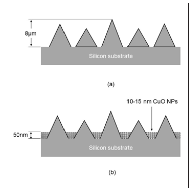
A silicon substrate of 8 cm in diameter and 300μm in thickness was etched using plasma etching system to produce surface roughness ranging in 3-8μm [15]. Copper oxide nanoparticles of 10-15nm particle size prepared by dc reactive sputtering technique were deposited on the silicon surface as a 50nm thin film. As an advantage of this technique, highly pure metal oxide nanoparticles can be synthesized. (Figure 1) shows schematically the proposed stages of this work. The spectral response of the prepared samples was measured in the spectral range 200-1200nm using a monochromator equipped with ceramic heater light source and chopper.
Figure 1:Schematic explanation of silicon surface before (a) and after (b) deposition of copper oxide nanoparticles.
Results and Discussion
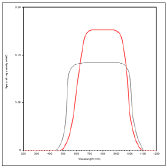
(Figure 2) shows the spectral response of the prepared samples before and after the deposition of copper oxide nanoparticles on the surface of silicon substrate. Before deposition of copper oxide nanoparticles, the silicon device shows typical response in the spectral range of 480-1080nm with a maximum response in the range of 720-880nm appearing as a plateau. After deposition of 50nm thin film of copper oxide nanoparticles, the spectral response was apparently increased. However, the spectral width was narrowed by ~50nm after deposition of copper oxide nanoparticles. The increase in the response may be ascribed to the matching of optical energy gap of both silicon (1.1eV) and copper oxide (1.2eV). Hence, the absorption of incident radiation is not affected. On the other hand, the narrowing in spectral response may be attributed to the quantum size effect of copper oxide nanoparticles as their response to the incident radiation is highly homogeneous and restricted to narrower region of spectrum. The difference in refractive index of silicon (3.5) and copper oxide (2.655) may contribute to the narrowing effect.
Figure 2: Spectral response of the silicon substrate before (black line) and after (red line) deposition of copper oxide nanoparticles.
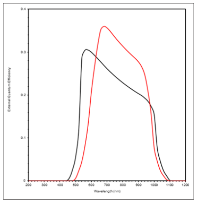
In order to introduce the effect of copper oxide nanoparticles on the photonic conversion of silicon device, the External Quantum Efficiency (EQE) was determined as a function of incident wavelength as shown in (Figure 3). The effect is clearly observed as the maximum efficiency was increased by 18% with a red shift of maximum wavelength from 580 to 680nm. Such effect can be successfully invested to enhance the performance of photonics and optoelectronics fabricated from these devices such photodetectors, optical switches, and couplers.
Figure 3:External quantum efficiency as a function of incident wavelength of the silicon substrate before (black line) and after (red line) deposition of copper oxide nanoparticles.
Conclusion
In concluding remarks, the deposition of copper oxide nanoparticles as thin film on the etched surface of silicon substrate may enhance the performance of the devices fabricated from such structures throughout increasing both spectral response and quantum efficiency and narrowing the spectral width. The whole process proposed in this work is highly reliable, highly reproducible, low in complexity and cost.
References
- Shainline JM (2021) Optoelectronic intelligence. Appl Phys Lett 118(14): 160501.
- Kneissl M (2020) A Short Introduction to Semiconductor Nanophotonics, in Semiconductor Nanophotonics. In: Kneissl M (Ed.), Springer, pp. 1-11.
- Zhou Z, Yin B, Michel J (2015) On-chip light sources for silicon photonics. Light: Sci Appl 4: e358.
- Liang D, Bowers JE (2010) Recent progress in lasers on silicon. Nat Phot 4: 511.
- Zhang C, Zhang J, Xiaohua M, Feng Q (2021) Silicon Solar Cells, Crystalline. Ch. 3, in Semiconductor Photovoltaic Cells, Springer, pp. 65-126.
- Tait AN, Ferreira de Lima T, Nahmias MA, Miller HB, Peng HT, et al. (2019) Silicon Photonic Modulator Neuron. Phys Rev Appl 11: 064043.
- Buckley S, Chiles J, McCaughan AN, Moody G, Silverman KL, et al. (2017) All-silicon light-emitting diodes waveguide-integrated with superconducting single-photon detectors. Appl Phys Lett 111(14): 141101.
- Hammadi OA (2015) Phot Sen 5: 152-158.
- Idjadi MH, Aatouni F (2020) Nature Photonics 14: 234-239.
- Hammadi OA, Khalaf MK, Kadhim FJ (2015) Opt Quantum Electron 47: 3805-3813.
- Miller SA, Chang YC, Phare CT, Shin MC, Zadka M, et al. (2020) Large-scale optical phased array using a low-power multi-pass silicon photonic platform. Optica 7(1): 3-6.
- Ismail RA, Abdulrazaq OA, Hadi AA (2007) Euro Phys J: Appl Phys 38: 197-201.
- Ismail RA, Abdulrazaq OA, Hadi AA (2005) Full characterization at 904nm of large area sip-n junction photodetectors produced by lid technique. Int J Mod Phys 19(31): 4619-4628.
- Hammadi OA, Naji NE (2016) Opt. Quantum Electron. 48: 375-381.
- Yousif AK, Hamadi OA (2008) Bulg J Phys 35: 191-197.
- Hammadi OA, Khalaf MK, Kadhim FJ (2016) Proc IMech E, Part N, J Nanomater, Nanoeng Nanosys 230: 32-36.
- Hammadi OA (2016) Characteristics of heat-annealed silicon homojunction infrared photodetector fabricated by plasma-assisted technique. Phot Sen 6: 345-350.
- Hamadi OA (2010) Profiling of antimony diffusivity in silicon substrates using laser- induced diffusion technique. Iraqi J Appl Phys Lett 3(1): 23-26.
© 2022 Oday A Hammadi. This is an open access article distributed under the terms of the Creative Commons Attribution License , which permits unrestricted use, distribution, and build upon your work non-commercially.
 a Creative Commons Attribution 4.0 International License. Based on a work at www.crimsonpublishers.com.
Best viewed in


.jpg)


 Editorial Board Registrations
 Submit your Article
 Refer a Friend
 Advertise With Us

.jpg)


.jpg)


.bmp)
.jpg)
.png)
.jpg)


.jpg)


.png)

.png)


.png)


