
- About Us
- Information
-

The Author ensures that the research has been conducted responsibly and ethically with adherence to all relevant regulations. read more..
- For Authors
- For Reviewer
- Manuscript Guidelines
- Membership
- Publication Ethics
-
- Journals
- Reprints
- e-Books
- Videos
- Policies
- Contact Us
 COVID-19
- Submissions


Full Text
COJ Electronics & Communications
The Effect of Selenium Source Temperature on the Structural Properties of Sb2Se3 Thin Films
Razykov TM1, Kuchkarov KM1, Ergashev BA1, Olimov A1 and Yuldoshov RT1,2*
1Physical-Technical Institute, Uzbek Academy of Sciences, Uzbekistan
2Tashkent Institute of Irrigation and Agricultural Mechanization Engineers, Uzbekistan
*Corresponding author: Yuldoshov RT, Physical-Technical Institute, Uzbek Academy of Sciences, Uzbekistan
Submission: June 15, 2023;Published: June 22, 2023

ISSN 2640-9739Volume2 Issue5
Opinion
Sb2Se3 is one of the best absorbent materials for next generation thin film solar cells and has excellent photovoltaic performance. Antimony selenide (Sb2Se3) is a promising alternative absorber material compared to the conventional thin film solar cells. Due to its outstanding properties, such as simple crystal structure, high absorption coefficient (>105sm−1), perfect optical band gap (1.1-1.3eV) and significant carrier mobility (~10sm2V-1s-1), Sb2Se3 has been regarded as one of the most attractive absorber candidates for the next-generation thin film solar cells. It should be noted that in the process of obtaining Sb2Se3 films by physical methods, a significant loss of Se occurs due to the process of decomposition of the films into Sb, Se, and SbSe during their synthesis. This leads to the formation of Se vacancies, which in turn increases the density of recombination centers in films [1]. This phenomenon negatively affects the optical and electrophysical properties of films and solar cells based on them. As being one of the most competitive absorber candidates for the next-generation thin film photovoltaic, Sb2Se3 has attracted much attention and so various deposition techniques; thus, thermal evaporation, Vapor Transport Deposition (VTD), Close-Spaced Sublimation (CSS) and sputtering [2] have been thoroughly studied to increase the PCE of the devices. The morphology and electrical properties of the films are found to be strongly dependent on the selenium source temperature, with higher temperatures resulting in larger crystalline grains and higher conductivity. These results suggest that the Chemical Molecular Beam Deposition (CMBD) method can be used to produce high-quality Sb2Se3 films with tunable properties for use in solar cell applications.
Experiment
Installed technological mode optimal cultivation quality Sb2Se3 films on surfaces glass (SLG-soda-lime glass) by the method chemical molecular beam deposition. The process of receiving Sb2Se3 films by the CMBD method was as follows: as original material used granules binary Sb2Se3 compound and Se semiconductor element purity (99.999%), which placed in different containers: Sb2Se3 into one and Se into the other. Further the system was brought to working condition and purged hydrogen for the purpose removal of atmospheric polluting gases. Dimensions samples -2.0×2.0cm2. For receiving Sb2Se3 film enriched selenium and stoichiometric composition, it was changed partial pressure Se in the steam phase in progress their growth. In this case temperature substrates were 500 °C, temperature sources elements varied in the ranges: 350 °С÷430 °С for Se and 700 °С for Sb2Se3, the rate growth amounted to 0.1÷1Å/sec at stream hydrogen WH2=20cm3/min. crystalline structure and phase compound materials explored method diffraction x-ray rays using-diffractometer. “Analytical Empyrean” on radiation CuK α(λ=1.5418Å) with a 2θ measurement in the range from 20° to 80° in 0.01° increments. Analysis phase composition produced using-Joint Committee on Powder Diffraction Standard (JCPDS) bases. Dark CVCs of Sb2Se3 films were measured using a Keithley 2420 Source Mete.
Result
Structural properties
were obtained at different selenium source temperatures. It can be seen from the X-ray patterns, that the total intensity of the (211), (221) peaks will sharply increase, while the (020), (230) and (240) peaks decrease at a selenium source temperature of 370 °C. Further increase in temperature to TSe=430 °C leads to a decrease in peaks (221), (211) and weak peaks (020), (120), (230) and (240) increase significantly. Additionally, for 2θ=29.66° for peak (101) low reflex detected intensity, indicating the formation of the Se phase (Figure 1). To quantitatively study the orientation of Sb2Se3 films, the Texture Coefficients (TC) of diffraction peaks were calculated based on the following equation.
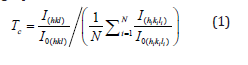
Figure 1:X-ray of Sb2Se3 films at different selenium source temperatures.

where I(hkl) and I0(hkl)-are the intensities of the diffraction peaks of the planes (hkl) on the measured and standard X-ray diffraction patterns of Sb2Se3 (JCPDS 15-0861), respectively. The large value of the TC of the diffraction peak indicates the predominant orientation in this direction. The TC values of the planes (hk0) of our samples tend to decrease at a selenium source temperature of 370 °С, and then begin to increase with a further increase in the selenium source temperature.
References
- Yuan C, Jin X, Jiang GS, Liu WF, Zhu CF (2016) Sb2Se3 solar cells prepared with salinized dc-sputtered metallic precursors. J Mater Sci 27: 8906-8910.
- Mavlonov A, Razykov T, Raziq F, Gan J, Chantan J, et al. (2020) A review of Sb2Se3 photovoltaic absorber materials and thin-film solar cells. Solar Energy 201: 227-246.
© 2023 Yuldoshov RT. This is an open access article distributed under the terms of the Creative Commons Attribution License , which permits unrestricted use, distribution, and build upon your work non-commercially.
Editor In Chief


.jpg)


Signup for Newsletter

Quick Links
 Editorial Board Registrations
 Submit your Article
 Refer a Friend
 Advertise With Us
Our Recent Edition

.jpg)


Top Editors


.jpg)


.bmp)
.jpg)
.png)
.jpg)


.jpg)


.png)

.png)


.png)


Financial Support

Sponsors

Latest e-Books

Latest Video

 a Creative Commons Attribution 4.0 International License. Based on a work at www.crimsonpublishers.com.
Best viewed in
a Creative Commons Attribution 4.0 International License. Based on a work at www.crimsonpublishers.com.
Best viewed in