
- About Us
- Information
-

The Author ensures that the research has been conducted responsibly and ethically with adherence to all relevant regulations. read more..
- For Authors
- For Reviewer
- Manuscript Guidelines
- Membership
- Publication Ethics
-
- Journals
- Reprints
- e-Books
- Videos
- Policies
- Contact Us
 COVID-19
- Submissions


Full Text
COJ Electronics & Communications
A Defected Microstrip Band Reject Filter by Multiple Tuneable Structures
Ansal KA*, Maheswary Sreenath, Arjun B Murali and Nina Cleetus
Department of Electronics and Communication, Saintgits College of Engineering, Kerala
*Corresponding author:Ansal KA, Department of Electronics and Communication, Saintgits College of Engineering, Kerala
Submission: June 22, 2022;Published: January 19, 2023

ISSN 2640-9739Volume2 Issue4
Abstract
A defected microstrip band reject filter by multiple tunable structures to sieve out the unwanted signal interferences in opposition to UWB systems especially narrowband is put forward and analyzed. A 50- Ohm microstrip band line is employed to obtain the anticipated defected microstrip band reject function. An oxbow notch (OBN), an inverted C-notch (ICN) and a horizontal cross notch (HCN) are incised on the substrate. Tuned measurements of the OBN, ICN, and HCN are selected to provide good tunable characteristics. The microstrip band reject filter is evaluated by the analogous circuit model and its simulations are presented for further analysis. The controllable center frequencies and miniature size are a few advantages of the reject filter obtained from the simulation and analysis results.
Keywords: Tunable reject filter; Defected microstrip-band structure; Oxbow notch; Horizontal cross notch; Impedance Characteristics; In-verted C-notch
Introduction
The introduction of UWB (Ultra Wide Band) technology provides benefits for various number of applications especially in public safety, businesses, industry and the consumers [1- 2]. However, the UWB systems may encounter with likely interventions which can be controlled by the introduction of defected ground structures like meander slots [3]. Thus, the defected ground structures like U-slot, V-slot, meander lines, arc shaped steps, split ring resonators, substrate integrated waveguide and much more are widely used in UWB applications [4- 9]. However, DMS (defected microstrip band structure) overcome the drawbacks of DGSs without any manipulation of the ground plane. DMS have properties of slow wave and thereby helps in the reject functioning of a filter. It is made by creating incisions in the form of slot patterns. It contributes to the reduction of size of the structure along with capacitance and inductance. Moreover, the defected microstrip structure has miniature size because it has excessive constructive inductance when compared with the defected ground structure. DMS is universally studied and utilized for filter designs and cross-talk reductions due to its merits. Most researchers put forward single or dual filtering bands. This paper discusses a defected microstrip band reject filter fabrication and measurements. Tunable structures are incorporated for the implementation of the filter. The defected tunable structures are incised on a 50- Ohm microstrip line. The DMS control the stop bands individually and obtain the anticipated function. The optimization of the proposed filter is done through HFSS. The S parameter characteristics, impedance characteristics, current distribution and the equivalent circuit were analysed in order to understand and evaluate the behavior of the filter. The simulation results provide us with the information that the filter imparts good performance within a miniature structure by the introduction of defected microstrip band structures.
Triple Stop Band Filter Design
The designed microstrip band reject filter configuration is shown in Figure 1. The recommended filter contains an oxbow notch (OBN), an inverted C-notch (ICN) and a horizontal cross notch (HCN) which is incised on a 50Ω microstrip line. Each defected microstrip structure cell checks on a stop-band, and therefore, these three bands are independently de- signed. Three bands are tuned using the DBMS theory. The microstrip band reject filter is incised on a Rogers RT/ Duroid 5880 substrate with 2.2 dielectric constant and 0.784mm thickness. The reject attributions of the defected microstrip structure are managed by varying the capacitance and inductance of the structure. The lower resonance of 3.5GHz is controlled by OBN, while the ICN regulates 5.2GHz bands. The upper resonance of 8.6GHz is regulated by the HCN and the high-order of DMS-1. Filter is simulated using ANSYS HFSS software version 19. The filter parameters are given in the Table 1.
Figure 1:Geometry of the proposed filter. (a) Front View (b) Back View (Ground)

Table 1: Filter Parameters.

Simulation Result
The simulation results are obtained using the ANSYS HFSS Electromagnetic solver. The analysed results of the proposed reject filter are S-parameter, current distribution and impedance characteristics. These outcomes are observed and the corresponding results are plotted.
A. S- Parameter
The scattering matrix parameters that show the relationship between the incoming and the outgoing reflected waves at the port junction are called S parameters. It provides transmission and reflection coefficient values for various studies concerned.
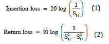
The simulation result, the S parameter of the proposed reject filter is as shown in the Figure 2. The bands obtained from the analysis are 3.5 GHz, 5.2 GHz and 8.6 GHz. The lower band of 3.5 GHz is affected by the OBN (DMS-1) while the middle stop band of 5.2 GHz is controlled by the ICN (DMS- 2). The upper frequency stop band of 8.6 GHz is affected by the HCN and the higher order of the DMS-1. The gains of these bands are - 19.51dB, -24.25dB, -18.09dB. The microstrip band reject filter provides enhanced performance for the systems with UWB applications especially from 3GHz - 9GHz.
Figure 2:S-parameter characteristics of microstrip band reject filter.

Impedance Characteristics
Impedance is the estimate of the combined dissent to flow of electricity in an AC circuit, comprising ohmic resistance and reactance. In complex form, Z = R c +iXc where Rc, ohmic resistance and Xc, reactance. Here, the impedance characteristics of the various bands are obtained as shown in the Figure 3.
Figure 3:Impedance characteristics.

Equivalent Circuit
The analogous circuit model is obtained for filter examination and proposed to affirm the efficacy of the simulation, which is achieved based on the Butterworth LPF (low-pass filter) theory. The simplest circuit model is given in Figure 4 compared to the Butter-worth LPF model.
Figure 4:Basic equivalent model of the DMS.

The impedance of the 1st Butterworth low-pass filter can be configured as:
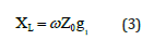
Where ω is the normalized angular frequency in which the filter operates, g1 is the normalized 1st Butterworth LPF parameter, Z0 is the characteristic impedance, 50 - Ohm. Then, the resonance of a simple DMS cell is:
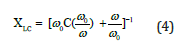
Where ω0 is the resonance frequency that is desirable given by the configured parallel inductance and capacitance. In order to simplify the inspection of the microstrip band reject filter, the above equation are equal when ω = ωc, where ωc denotes the cutoff frequency of the parallel LC resonator and is illustrated in the Figure 5.
Figure 5:Equivalent circuit of the reject filter.

Current Distribution
The current distribution provides the signal performance which aids in optimizing the system characteristics. The current distribution of the proposed defective reject filter at a solution frequency of 5.2GHz is as shown in the Figure 6. At this frequency the current distribution is almost uniform.
Figure 6:Current distribution at the solution frequency 5.2GHz. (a) Top View (b) Bottom View

Conclusion
Microstrip band reject filter by using defected microstrip structure has been developed and its performance is analysed by Ansys 16 (HFSS). The microstrip band reject filter is compact in size when it is compared with the previous filters designed for the reject application in various aspects. Besides, the designed defective microstrip band filter is designed easily, and resultant frequencies and bandwidth of the microstrip band reject filter can be regulated in individual. Hence this design provides the users a large amount of liability and wide utilization. The interpretation of the designed filter is done through inspect of equivalent circuit, HFSS design, current distributions, impedance characteristics and the S - parameter characteristics.
References
- Sharma K (2018) CPW-Fed UWB Reconfigurable Antenna (RF MEMS Switch) with X Band Applications. 6th (Edn), of International Conference on Wireless Networks & Embedded Systems (WECON), Rajpura, India, pp. 37-40.
- Naser Ojaroudi Parchin, Haleh JB, Yasir IA Al Yasir, Raed A Abd Alhameed, Ahmed M Abdulkhaleq, et al. (2019) Recent Developments of Reconfigurable Antennas for Current and Future Wireless Communication Systems. Electronics 8(2): 128.
- Chen SY, Chu QX, Shinohara NA (2016) A bandwidth reconfigurable planar antenna for WLAN/WiMAX applications. In Proceedings of the Asia-Pacific Microwave Conference (APMC), New Delhi, India, pp. 5-9.
- Shakhirul MS, Jusoh M, Lee YS, Husna (2018) A Review of Reconfigurable Frequency Switching Technique on Micostrip Antenna. J Phys Conf Ser 1019: 012042.
- Yanzhuang Yin, Mingming Lv, Long Ma, Xubao Sun (2019) Research on the Development of Frequency Reconfigurable Antenna and Polarization Reconfigurable Antenna. IOP Conference Series: Earth and Environmental Science 242: 022051.
- Yao C, Longfang Y, Jianliang Z, Yanhui L, Liang Z, et al. (2017) Frequency Reconfigurable Circular Patch Antenna with an Arc-Shaped Slot Ground Controlled by PIN Diodes. International Journal of Antennas and Propagation 2017: 7081978.
- Mansoul Ali, Kimouche, Hocine (2013) A simple frequency reconfigurable µ-band patch antenna for wireless communication. pp. 306-309.
- Rakshitha V, Nikky Kumari, Bhavana B, Ravikant Rai (2016) Frequency Reconfigurable Antenna. International Journal of Engineering Research & Technology (Ijert) ICACT 4(22): 1-4.
- Yingsong Li, Shengyuan Luo, Wenhua Yu (2018) A Compact Tunable Triple Stop-Band Filter Based on Different Defected Microstrip Structures. ACES Journal 33(7): 752-757.
© 2023 Ansal KA. This is an open access article distributed under the terms of the Creative Commons Attribution License , which permits unrestricted use, distribution, and build upon your work non-commercially.
Editor In Chief


.jpg)


Signup for Newsletter

Quick Links
 Editorial Board Registrations
 Submit your Article
 Refer a Friend
 Advertise With Us
Our Recent Edition

.jpg)


Top Editors


.jpg)


.bmp)
.jpg)
.png)
.jpg)


.jpg)


.png)

.png)


.png)


Financial Support

Sponsors

Latest e-Books

Latest Video

 a Creative Commons Attribution 4.0 International License. Based on a work at www.crimsonpublishers.com.
Best viewed in
a Creative Commons Attribution 4.0 International License. Based on a work at www.crimsonpublishers.com.
Best viewed in