
- About Us
- Information
-

The Author ensures that the research has been conducted responsibly and ethically with adherence to all relevant regulations. read more..
- For Authors
- For Reviewer
- Manuscript Guidelines
- Membership
- Publication Ethics
-
- Journals
- Reprints
- e-Books
- Videos
- Policies
- Contact Us
 COVID-19
- Submissions


Full Text
COJ Electronics & Communications
CFOA based Integrator Suitable for Analog Signal Processing
Praween K Sinha*, Mohit Kumar, Gautam Kunal Haruray and Neelam Sharma
Department of Electronics and Communication Engineering, Maharaja Agrasen Institute of Technology, India
*Corresponding author: Praween K Sinha, Department of Electronics and Communication Engineering, Maharaja Agrasen Institute of Technology, Sec-22, Rohini, New Delhi-110086, India
Submission: August 25, 2018;Published: October 30, 2018

ISSN 2640-9739 Volume1 Issue3
Abstract
Current Feedback Operational Amplifier (AD844) uses a circuit design that emphasizes current-mode operation, which is inherently much faster than voltage-mode operation because it is less effected by stray node-capacitances. When fabricated using high-speed complementary bipolar processes, CFOA’s can be orders of magnitude faster than other available feedback amplifiers ex. VFA’s. With CFOAs, the amplifier gain may be controlled independently of bandwidth. All these constitutes the major advantages of CFOAs. Some new and more efficient active RC integrator circuit realizations, using minimum passive components grounded and a current feedback operational amplifier (CFOA) device are proposed. Integrator with Grounded passive components allow better usability in VLSI. Finally, experimental result by wave processing has been verified using Proteus software.
Keywords: Integrators; Current-feedback-operational-amplifiers; Current mode circuits
Introduction
Active - RC integrator circuit is widely used in analog computers, analog-to-digital converters and wave-shaping circuits. These circuits essentially fuse a ratio type (y1/y2) function involving an active device like the voltage operational amplifier, operational trans-conductance amplifier, current conveyor, and current feedback operational amplifiers [1-6]. But use of Current Feedback Operational Amplifier’s has increased exponentially in past few years [3-5] because of the its distinctive characteristics, in comparison with traditional operational amplifiers, like inverting input with low input resistance, additional output with high output resistance, frequency range extension, and very fast large signal response (major advantages over the op-amp are the increased device bandwidth at higher slew-rate, and, accurate port tracking properties leading to a less sensitive design) [7-13]. Typically, these amplifiers perform on the complementary bipolar technology on heterogeneous symmetric p-n-p and n-p-n transistors. Experimental results on wave processing have been verified with Proteus simulation.
CFOA
Figure 1:Current feedback operational amplifier (AD844).

The current feedback operational amplifier (CFOA) is a type of electronic amplifier which have current as inverting input, rather than voltage as in a conventional voltage-feedback operational amplifier (VFA). Figure 1 gives a representation of the amplifier with potential (Y) and current (X) inputs and potential (O) and current (Z) outputs. A CFOA is a four terminal building block characterized by the following terminal equations.
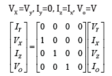
These circuits showcase better performance, particularly higher speed and better bandwidth, than voltage mode operational amplifiers (VOA). The current feedback operational amplifier (CFOA) close-loop bandwidth is independent of its close-loop gain (provided that the feedback resistance is kept constant and much higher than the CFOA inverting input resistance) unlike VOAbased circuits, which are limited by a constant gain-bandwidth product. The CFOA block is preferred for low-voltage, low-power applications and is characterized by low voltage-transfer errors and high output driving current capability [1].
In this paper, new circuit models are developed by giving appropriate basic thought to the subject all in current mode. As a result, new integrator circuits have been developed having efficient performance and characteristics. New sets of circuit models based on current mode approach, which have been developed are likely to find productive use in the field of modern electronics. This work offers some circuits having improved characteristics with respect to tenability, component count, integrability i.e. chip area economization. These circuits can be of great value in signal processing, communication and instrumentation area.
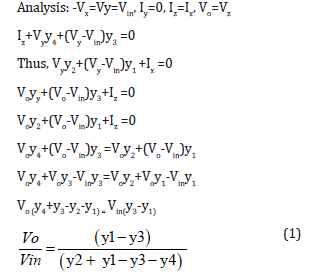
Generalised Scheme hor Generation of Different Types of Integrators
Mathematical Analysis
Integrator: Figure 2
Figure 2:integrator.

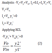
Integrator 1: Figure 3
Figure 3:Integrator 1.

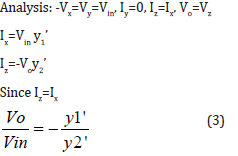
Integrator 2: Figure 4
Figure 4:Integrator 2.

Practical Working Cases
Case I (Integrator 1) Figure 5
Figure 5:Schematic diagram case I.

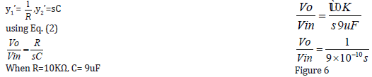
Figure 6:Simulation of case I.

Wave conversion at 10Hz by CFOA of Figure 5 using R=10KΩ, C=9uF
Case II (Integrator 2) Figure 7
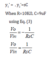
Figure 7:Schematic of case II.

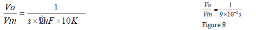
Figure 8:Simulation of case II.

Case III (Integrator) Figure 9
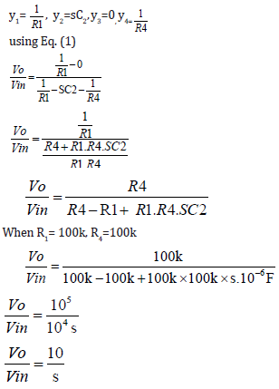
Figure 9:Schematic of case III.

Figure 10:Simulation of case III.

Wave conversion at 10Hz by CFOA of Figure 7 using R=10KΩ, C=9uF.
Wave conversion at 10Hz by CFOA of Figure 9 using R1=100kΩ, R4=100kΩ
Case IV (Integrator 2) Figure 11
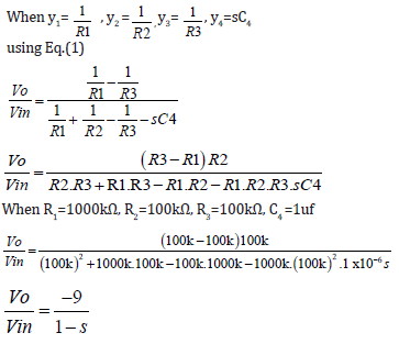
Figure 11:Schematic of case IV.

Figure 12:Simulation of case IV.

Wave conversion at 10 Hz by CFOA of Figure 11 using R1=1000kΩ, R2=100kΩ, R3=100kΩ , C4=1uf
Case V (Integrator 3) Figure 13
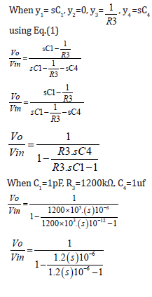
Figure 13:Simulation of case V.

Figure 14:Simulation of case V.

Figure 14
Wave conversion at 10Hz by CFOA of Figure13 using C1=1pF, R3=1200kΩ, C4=1uf.
Figure 15:Simulation of case VI.

Case VI (Integrator 4) Figure 15
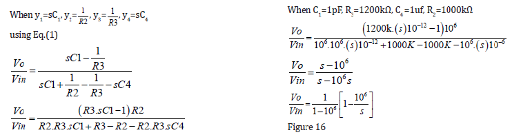
Figure 16:Simulation of case VI.

Wave conversion at 10Hz by CFOA of Figure15 using When C1=1pF, R3=1200kΩ, C4=1uf, R2=1000kΩ
Experimental Result
All the proposed configurations had been tested with Proteus simulation. The AD-844 CFOA was used as the active device. In our experiments, regulated bias voltages were set at 0±12Vdc. for the CFOA. Time domain tests for wave conversion measurement were carried out. Some typical results on wave conversion by the integration functions are shown in Table 1. For these tests, the input signals were square wave for the integrators. The gain and frequency had been measured from the oscilloscope display on Proteus simulation. The proposed circuits exhibited satisfactory response practically expected from an integrator.
Table 1:Results (Practical and theoretical values).

Conclusion
In this paper, an analysis and simulation is presented about six new cases of active RC integrator circuit realizations, using minimum passive components grounded and a current feedback operational amplifier (CFOA) device are proposed. Integrator with grounded passive components allows better usability in VLSI. The realizability equations are derived and experimental result by wave processing has been verified using Proteus software. The proposed circuits exhibited satisfactory response as practically expected from an integrator.
References
- Nagaria RK (2008) On the new design of CFA based Voltage Controlled Integrator/Differentiator suitable for analog signal processing. WSEAS Transaction on Electronics 6: 232-237.
- Sanyal SK, Sarker UC, Nandi R (1990) Increased time constant dualinput integrators. IEEE Trans on Instrumentation and Measurement 39(4): 672-673.
- Minaei S, Topcu G, Cicekoglu O (2003) Active only integrator and differentiator with tunable time constants. International Journal of Electronics 90(9): 581-588.
- Minaei S (2004) Simple DVCC-based current mode integrators and differentiator Frequenz. Journal of Telecommunication 58(1-2): 41-45.
- Liu SI, Hwang YS (1994) Dual-input differentiators and integrators with tunable time constants using current conveyors. IEEE Trans on Instrumentation and Measurement 43(4): 650-654.
- Minaei S, Sayin OK, Kuntman H (2006) A new CMOS electronically tunable current conveyor and its application to current mode filters. IEEE Transactions on Circuits and Systems 53(7): 1448-1457.
- Venkateswaran P, Nandi R, Das S (2012) New integrators and differentiators using a MMCC. Circuits and Systems 3: 288-294.
- Senani R (1998) Realization of a class of analog signal processing/ signal generation circuits, novel configurations using current feedback operational amplifier. Frequenz 52(9): 196-206.
- Singh AK Senani R (2001) Active R design using CFOA-poles: New resonators, filters and oscillators. IEEE Trans on Circuits and Systems-II 48(5): 504-511.
- Maundy B, Gift SJG, Aronhime PB (2004) A novel differential high frequency CFA integrator. IEEE Trans on Circuits & Systems-I 51(6): 289-293.
- Toumazou C, Lidgey J (1994) Current feedback opamps; A blessing in disguise. IEEE Circuits and Dev Mag 10(1): 34-37.
- Ismail AM, Soliman AM (2000) Novel CMOS current feedback Op-Amp realization suitable for high frequency applications. IEEE Trans Circuit Syst I 47(6): 918-921.
- Mita R, Palumbo G, Pennisi S (2005) Low voltage high drive CMOS Current feedback op-amp. IEEE Trans Circuit Syst II 52(6): 317-321.
© 2018 Praween K Sinha. This is an open access article distributed under the terms of the Creative Commons Attribution License , which permits unrestricted use, distribution, and build upon your work non-commercially.
Editor In Chief


.jpg)


Signup for Newsletter

Quick Links
 Editorial Board Registrations
 Submit your Article
 Refer a Friend
 Advertise With Us
Our Recent Edition

.jpg)


Top Editors


.jpg)


.bmp)
.jpg)
.png)
.jpg)


.jpg)


.png)

.png)


.png)


Financial Support

Sponsors

Latest e-Books

Latest Video

 a Creative Commons Attribution 4.0 International License. Based on a work at www.crimsonpublishers.com.
Best viewed in
a Creative Commons Attribution 4.0 International License. Based on a work at www.crimsonpublishers.com.
Best viewed in