
- About Us
- Information
-

The Author ensures that the research has been conducted responsibly and ethically with adherence to all relevant regulations. read more..
- For Authors
- For Reviewer
- Manuscript Guidelines
- Membership
- Publication Ethics
-
- Journals
- Reprints
- e-Books
- Videos
- Policies
- Contact Us
 COVID-19
- Submissions


Full Text
COJ Electronics & Communications
Performance Analysis of CNFET Based 6T SRAM
Divya1, Manjit Kaur2 and Gurmohan Singh3*
1 Research Scholar, C-DAC Mohali, India
2 Senior Engineer, C-DAC Mohali, India
3 Principal Engineer, C-DAC Mohali, India
*Corresponding author: Gurmohan Singh, Principal Engineer, C-DAC Mohali-160071, India
Submission: July 26, 2018;Published: September 24, 2018

ISSN 2640-9739 Volume1 Issue2
Abstract
CNFET is an emerging device which facilitates continuing feature size scaling trend. This novel device is predicted to outperform existing planer devices in near future owing to its unique features like ballistic transport operation, excellent carrier mobility, high current carrying capability, high stability, one dimensional band structure. In this paper, the performance of CNFET based six transistor (6T) SRAM cell has been analyzed. The effects of variations in dielectric material, oxide thickness, metal gate and CNT work function, Fermi level and chiral vector on power delay product (PDP) and static noise margin (SNM) are comprehensively analyzed. It is observed that Hafnium Silicate (HfSiO4) as dielectric material at 1nm oxide thickness yields best results in terms of stability and energy efficiency. CNT work function of 4.65eV yields most optimum PDP value of 63.59 zepto Joule. The optimum SNM value of 358mV has been obtained at a CNT work function of 4.28eV along with best PDP/SNM ratio of 5.6mV/zJ. It is also observed that Fermi level at 0.6eV gives the most promising results. The computed results indicate that (22, 0) chirality based 6T SRAM cell yield the best performance from energy efficiency point (PDP) of view along with highest SNM/PDP ratio of 6.30mV/zJ. To get more stable SRAM cell, (13, 0) chirality gives the best SNM result of 381mV.
Keywords: CNFET; CNT; MOSFET; PDP; SNM; 6T SRAM; SCE
Introduction
According to Moore’s law, device dimensions are continually scaled down to nanometer regime which resulted in short channel effects (SCEs), drain induced barrier lowering (DIBL), static power dissipation, threshold voltage roll-off and band to band tunneling (BTBT) [1]. The use of thinner gate oxide and high-k dielectric material helps to eliminate this problem due to increase in gate capacitance [2]. According to International Technology Roadmaps for Semiconductors (ITRS) [3], new material and devices are required that can be integrated with the current silicon-based technology in near future. The silicon on insulator (SOI) MOSFET, Multiple-gate field-effect transistor (MGFET), FinFET [4], Tunnel FET [5], Nanowire FET [6], Single electron transistor (SET) [7], and CNFETs [8-11] are the emerging solutions to planar bulk MOSFETs providing better control on the drain potential over the channel. The best replacement for silicon is semiconducting CNTs because of their properties like lower power consumption, near-ballistic operation, reduced short channel effects, high carrier mobility, one dimensional band structure, higher operating frequencies and improved electrostatics at nanoscale due to its non-planar structure [12,13].
Silicon dioxide can be replaced by high-k dielectric material for gate insulators to reduce direct tunneling leakage currents as it provides efficient charge injection into transistor channels. Scaling down the device dimensions also scales the oxide thickness which leads to sharp increase in leakage current in case of MOSFET [14]. It is observed that CNFET is a candidate transistor for low power, energy efficient and stable design. The ballistic transport of CNT reduces collisions of charge carriers in CNFET which results in the power reduction. Doping level is determined by the Fermi level of doped region in CNFET. The threshold voltage of CNFET depends on the diameter or chiral vector of CNT [15].
Deng et al. [16,17] proposed the circuit compatible HSPICE model for CNFET in the intrinsic channel region including the nonidealities. This model allows changing various parameters like chirality, no. of tubes, dielectric constant, oxide thickness, work function, Fermi level etc. Sinha et al. [18] investigated the impact of dielectric thickness on gate capacitance of various devices i.e. MOSFET, Nanowire FET, and CNFET devices and examined that CNFET gives better results than MOSFET. Das et al. [19] analyzed that drain induced barrier lowering parameter reduces at lower oxide thickness and high-k dielectric material. Kumar et al. [20] analyzed the effect of variation of dielectric material and dielectric thickness of gate insulator on current voltage characteristics of CNFET and observed that thinner gate oxide and high-k dielectric material have improved the device performance. Kaur et al. [21] evaluated the effect of dielectric variation and oxide thickness on the performance of CNFET based logic gates and observed that hafnium silicate and oxide thickness of 2nm gives optimal results in terms of PDP. Shirazi et al. [22] analyzed the performance dependence of CNFET on doping level at different diameters. Kohli et al. [23] analyzed the effect of variation of work function of contact metal on NCNFET and observed that aluminum as contact metal gives the better results in terms of I-V characteristics. Sheng Lin contemplated the design and analysis of CNFET based SRAM and TCAM cells by varying the diameter of CNT [24,25]. Sethi et al. [26] presented design and performance analysis of CNFET based TCAM Cell by dual chirality selection. Emon et al. [27] proposed the design of SRAM cell using CNFETs which shows the improvement in power and static noise margin by 37.2% and 40.6%.
In this paper, we comprehensively evaluated the influences of the various parameters such as dielectric material, oxide thickness, Fermi level, chiral vector, metal gate and CNT work function fluctuations on CNFET based 6T SRAM cell design. This paper is organized as follows: Section II presents materials and methods describing CNFET structure proposed by Stanford University and investigates its I-V characteristics along with design and operation of CNFET Based 6T SRAM Cell. Section III presents results and discussions. Conclusions are covered in Section VI.
Materials and Methods
Carbon nanotubes are the basic element of CNFETs and discovered by Sumio Iijima in 1991. CNTs are the allotropes of carbon made up by rolling the sheet of graphene in the form of cylinder. Graphene is a one atom thick sheet of graphite having honeycomb lattice structure. Their electronic and atomic structure gives a unique advantage as FET channel which includes long mean free paths (i.e. ballistic transport) and low scattering of carriers. The first CNFET was testified in 1998. CNFET has the same structure as MOSFET, only the CNT that can be either a single wall (SWCNT) or multiwall (MWCNT) is used as a channel of transistor. Due to high current carrying capability, SWCNTs are usually preferred. They are formed by one or more semiconducting CNTs perfectly aligned and a well-positioned whose section under the gate is intrinsic and the semiconductor extension regions are n/p doped as shown in Figure 1. CNFETs have various favourable electrical properties such as superior subthreshold slope, high transconductance, high mobility, high current density, less band gap, ballistic transport, superior threshold voltage, high on-to-off (Ion/Ioff) current ratio.
Figure 1:(a) Cross-sectional view of a CNFET structure, and (b) Top view.

CNFETs are categorized as Schottky barrier CNFET, conventional CNFET, partially gated CNFET and tunnel CNFET. The Stanford CNFET model is used in this work which is a MOSFET like CNFET compact model. It is a universal circuit compatible HSPICE model which includes various non-idealities such as screening effect caused by multiple CNTs and scattering in the channel region. This model has been investigated in this work for variation in dielectric material and its thickness, metal gate and CNT work function, Fermi level and chiral vector. The I-V characteristics of NCNFET are shown in Figure 2 which represents the relationship between drain current (IDS) and drain to source voltage (VDS).
Figure 2:I-V characteristics of (a) NMOS (b) NCNFET at 16nm technology node.

SRAM is a volatile memory i.e. memory in which the data in the cell remains constant only if the power is applied. It is the commonly used on-chip memory. Due to low power operation, more robustness and short access time, 6T SRAM cell is normally used. It uses a pair of cross-coupled inverters to retain its state and two access transistors one for each bit-line as shown in Figure 3. Feedback is used to reduce the disturbances caused due to leakages and noise. When a high signal is applied to the word line (WL), the SRAM cell is activated and read or write operation is performed through bit lines (BL and BLB) [28-30].
Figure 3:CNFET based Schematic design of 6T-SRAM Cell.

Stability of SRAM cell is important as it determines the soft error rate i.e. the rate at which the data saved in the memory cell gets corrupted. Static Noise Margin (SNM) is the key performance metric for the stability of SRAM cell. Further, an SRAM cell needs to be sufficiently stable during the read operation. Also it should be easy to write any data to it during write operation. SNM is the minimum noise voltage that is required to flip the state of the cell. SNM can be calculated graphically by drawing the voltage transfer characteristics (VTC) of the both the inverters of SRAM cell. Power Delay Product (PDP) is another figure of merit to determine the performance of SRAM cell. This parameter is used to calculate the energy efficiency of the cell. The speed at which the gate capacitors of transistor stores energy is used to determine propagation delay. To transfer energy at high speed, high power consumption is required. Power and propagation delay form a design trade-off. So, the combine metric is used to determine the performance of the circuit. Lower PDP makes the circuit faster and energy efficient. For a fast, stable and power efficient design, lower write time, high SNM and less average power are required. Therefore, the ratio of SNM to PDP is used to obtain best overall performance of SRAM cell.
Results and Discussion
Influence of dielectric material
Since 1959, when MOSFET was invented, the material used as gate dielectric was silicon dioxide having low dielectric constant i.e. 3.9. The reason behind choosing it is due to its electrical and thermal stability interface between silicon (as substrate) and silicon dioxide (as dielectric). To achieve high speed and lesser chip area, gate length and physical thickness of silicon dioxide need to be scaled. But as a result, due to direct tunneling of electrons through silicon dioxide, gate leakage will be high leading to significant increase in circuit power dissipation. It is difficult to control gate over the channel because of strong electrostatic coupling between drain and source electrodes. The key solution of this problem is to use high-k dielectric material at lower device dimensions which gives high gate capacitance. The unique advantage of CNFETs is that they are compatible with high-k dielectrics.
In this paper, the value of dielectric constant is varied from 3.9 to 30. CNFET based 6T SRAM cell is simulated for different dielectric materials such as Silicon dioxide (SiO2), Aluminum Oxide (Al2O3), Hafnium Silicate (HfSiO4), Hafnium Oxide (HfO2), Zirconium Oxide (ZRO2) and Lanthanum Oxide (La2O3) at dielectric thickness of 1nm. The (Figure 4A-C) illustrate the computed results for CNFET based 6T SRAM cell for different dielectric materials in terms of PDP, SNM and SNM/PDP ratio. The PDP index represents energy efficiency and switching speed of a digital circuit, whereas SNM and SNM/PDP ratio are indicative of stability of a digital circuit. It is observed that HfSiO4 dielectric yields the best performance with PDP of 73.22 zepto Joule, SNM of 361mV along with highest SNM/ PDP ratio of 4.93mV/zJ. The SiO2 exhibits worst performance with PDP of 142.31 zepto Joule and SNM/PDP ratio of 2.42mV/zJ among all dielectric materials. The HfO2 exhibits the worst SNM value of 326mV.
Figure 4:(a) Comparison of PDP results, (b) SNM results, and (c) SNM/PDP ratio for CNFET based 6T SRAM cell for different dielectric materials.

Influence of oxide thickness
Oxide thickness is the thickness of the dielectric material (insulator) between gate and channel. To increase the conductivity when the transistor is in on-state dielectric thickness should be less. In case of MOSFET, as the device dimension scales down, the thickness of gate dielectric material is continually decreasing, and capacitance is increasing and so drive current, raising the device performance. When the thickness goes below 1.5nm, direct tunneling starts increasing rapidly which leads to higher power consumption and degrades the reliability. High-k dielectric materials can be used to reduce the tunneling but they increase quantum capacitance effect while maintaining thicker oxide layer. Quantum capacitance is an important parameter in nano-scaled devices as the movement of Fermi level depends on it. So, to overcome these problems MOSFETs are replaced with CNFETs, as it has the property of reducing quantum capacitance by decreasing oxide thickness which leads to less leakage and improved performance.
Figure 5:(a) Bar-graph comparison of PDP results, (b) SNM results, and (c) SNM/PDP ratio for CNFET based 6T SRAM cell for thickness variation of SiO2 and HfSiO4 dielectric materials.

The value of oxide thickness is varied from 1 to 4nm. CNFET based 6T SRAM cell is analyzed for SiO2 and HfSiO4 as dielectric material for different oxide thicknesses. The Figure 5A-5C illustrate comparative bar-graphs for CNFET based 6T SRAM cell for thickness variation of SiO2 and HfSiO4 dielectric materials in terms of PDP, SNM and SNM/PDP ratio. The results reveal that HfSiO4 with 1nm oxide thickness yield the optimum PDP of 73.220 zepto Joule, SNM of 361mV, and SNM/PDP ratio of 4.93mV/zJ.
Influence of work function
In solid state electronics, work function is an important parameter as it signifies the minimum energy required to free the electron at the surface of the solid. When there is a junction involved with metal, it becomes important to consider the work function of material. For metal gate devices, it is important to choose a metal element which satisfies a suitable work function (as it determines the threshold voltage) and the thermal stability. The work function of the metal must be between conduction band and valence band of silicon. Due to gate depletion effect, thermal instability and low conductivity with high-k dielectric materials, the conventional polysilicon gate is less used nowadays. In this paper, the value of metal gate work function is varied from 4.1 to 5.1eV at constant CNT work function of 4.5eV. CNFET based SRAM cell is simulated for different metal gates such as N+Polysilicon (N+ Poly), Tantalum (Ta), Aluminum (Al), Copper (Cu) and Gold (Au) with work function values of 4.1, 4.25, 4.28, 4.65 and 5.1eV respectively. From the results it can be observed that there is a negligible variation in PDP results for different gate materials and exhibit no variations in SNM results. The Figure 6 depicts the bar-graph comparison of PDP results for different gate materials.
Figure 6:Effect of gate material variations on PDP of CNFET based 6T SRAM cell..

Figure 7:Effect of CNT work function variations on PDP and SNM results of CNFET based 6T SRAM cell.

CNT work function is another important parameter to control the field emission properties of carbon nanotube. It plays an important role in controlling carrier transport through the nanotube when it forms the junction and reduces the threshold voltage. In this paper, the value of CNT work function is varied from 4.1 to 5.1eV at constant metal gate work function of 4.5eV. CNFET based SRAM cell is simulated for different work function values of 4.1, 4.25, 4.28, 4.65 and 5.1eV respectively. From computed results for CNFET based 6T SRAM cell, it can be observed that at CNT work function of 4.65 eV yield most optimum PDP value of 63.591 zepto Joule. The optimum SNM value of 358 mV has been obtained at a CNT work function of 4.28 eV along with best PDP/SNM ratio of 5.6mV/zJ. It is also observed that CNT work function value of 4.10 eV exhibits worst results for PDP, SNM, and SNM/PDP ratio. The Figure 7 depicts the PDP and SNM results for different CNT work function values.
Effect of variation in fermi level
For determining the performance of CNFET, an optimal Fermi level should be chosen which depends on doping level. With no doping, Fermi level is exactly at the center of band gap. As doping rate is increased, the Fermi level moves towards the conduction band which in turn reduces the barrier height. Fermi level of channel is assumed to stay along the Fermi level of source which means that the energy band diagram of the channel is pushed down due to which potential barrier height between the channel and source reduces. In this paper, CNFET based 6T SRAM cell is analyzed for four values of Fermi level i.e. 0.4, 0.5, 0.6 and 0.7 eV. From the computed results, it is observed that there is no variation in SNM but from PDP point of view, 0.6 eV Fermi level gives the best results. The Figure 8 illustrates the computed PDP results for CNFET based 6T SRAM cell at different Fermi levels.
Figure 8:Computed PDP results of CNFET based 6T SRAM cell at different Fermi levels.

Effect of variation in chiral vector
Chiral vector is an important parameter of nanotubes as it defines the orientation of hexagonal structure with respect to longitudinal axis of nanotube. Depending upon this structural arrangement, a CNT can behave like a conductor or semiconductor. The chiral vector can be represented by an integer pair (n, m). The sheet of graphite is rolled up and joined together with a wrapping vector (C) to form a CNT. The wrapping vector (C) or the circumference of CNT can be expressed as given in equation (1)
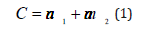
Where, a1 and a2 are unit lattice vectors, n and m are integers that represent the chirality of nanotube. SWCNT can exhibit either metallic or semiconducting behavior depending on the chiral number which decides electrical properties of the CNT. It is metallic if (nm) is divisible by 3 or n is equal to m; otherwise it is semiconducting if (nm) is not divisible by 3. CNFETs utilize semiconducting CNTs. The chiral vector (nm) of CNT determines various parameters such as diameter, threshold voltage, shape and size of brillouin zone. The diameter of CNT (DCNT) can be expressed by equation (2).
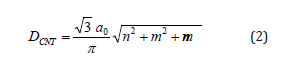
Where a0=0.142nm is inter-atomic distance between each carbon atom and its neighbor. From Figure 9, it is observed that as chiral vector increase, the diameter of CNT also increases.
Figure 9:Diameter of CNT at different chiral vectors

Chiral angle (θ) represents the direction of chiral vector, which can be determined by equation (3)
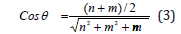
The variation in nanotube properties occurs due to variation in chiral angle (θ) and diameter (DCNT). The threshold voltage (VTH) is the minimum voltage required to turn on the transistor and for CNFET it can be expressed by equation (4).
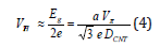
Where, Eg is bandgap energy, e is charge on an electron, a=2.49Å is carbon to carbon atom distance, Vπ=3.033eV is carbon π to π bondsss energy in tight bonding model and DCNT is diameter of CNT. From equation (4), it is clear that as diameter of CNT changes, the threshold voltage also varies as shown in Figure 10. The threshold voltage of NCNFET is same as PCNFET at same chiral vector but opposite in polarity.
Figure 10:Computed PDP results of CNFET based 6T SRAM cell at different Fermi levels.

In this paper, the diameter of CNT is varied from 0.783 to 1.722nm. CNFET based 6T SRAM cell is analyzed at different chiral vectors such as (10, 0), (13, 0), (16, 0), (19, 0) and (22, 0). From computed results in Table 1, it can be observed that (22, 0) chirality-based SRAM cell gives the best performance from energy efficiency point (PDP) of view along with highest SNM/PDP ratio of 6.30mV/zJ. To get more stable SRAM cell, (13, 0) chirality gives the best SNM result of 381mV.
Table 1:SNM and PDP results of 6T SRAM cell at different chiral vectors.

Table 2 shows the comparison of various CNFET based memory cell structures with proposed design. Compared to various designs [24,26-28] the proposed SRAM cell is best in terms of performance efficiency (PDP) and stability index (SNM). CMOS based SRAM cell is also designed at 16nm technology node to analyze and compare its results with CNFET counterpart. Table 3 shows the comparison of CMOS and CNTFET based 6T SRAM cell design. It is observed that PDP and SNM of CNTFET based SRAM cell design are better than CMOS based design.
Table 2:Comparison of various CNTFET based memory cells.

Table 3:Comparison of CMOS and CNTFET based SRAM cells.

Conclusion
This paper evaluates energy efficiency, delay, and stability related parameters of a CNFET based 6T SRAM cell structure and comprehensively analyzes the effect of variations in various parameters. The results revealed that HfSiO4 dielectric yields the best performance with PDP of 73.22 zepto Joule, SNM of 361mV along with highest SNM/PDP ratio of 4.93mV/zJ. The value of oxide thickness is varied from 1 to 4nm for SiO2 and HfSiO4 as dielectric materials. The results revealed that HfSiO4 with 1nm oxide thickness yield the optimum PDP of 73.220 zepto Joule, SNM of 361mV, and SNM/PDP ratio of 4.93mV/zJ. The value of metal gate work function is varied from 4.1 to 5.1eV at constant CNT work function of 4.5eV. However, the CNT work function of 4.65eV yields most optimum PDP value of 63.591 zepto Joule. The optimum SNM value of 358 mV has been obtained at a CNT work function of 4.28eV along with best PDP/SNM ratio of 5.6mV/zJ. Also, CNFET based 6T SRAM cell is analyzed for four values of Fermi level i.e. 0.4, 0.5, 0.6 and 0.7eV and it is observed that there is no variation in SNM but from PDP point of view, 0.6eV Fermi level gives the best results. The computed results indicate that (22, 0) chirality-based SRAM cell gives the best performance from energy efficiency point (PDP) of view along with highest SNM/PDP ratio of 6.30mV/zJ. To get more stable SRAM cell, (13, 0) chirality gives the best SNM result of 381mV.
References
- Taur Y, Buchanan Da, Chen W, Frank DA, Ismail KE, et al. (1997) CMOS scaling into the nanometer regime. Proceedings of the IEEE 85(4): 486- 504.
- Taur Y (1999) The incredible shrinking transistor. IEEE Spectrum 36(7): 25-29.
- International technology roadmap for semiconductors.
- Dani LM, Singh G, Kaur M (2015) FinFET based 6T SRAM cell for nanoscaled technologies. International Journal of Computer Applications 127(13): 5-10.
- Kaur G, Singh G, Kaur M (2016) Double gate heterostructure based tunnel FET with 51.5mV/decade subthreshold slope. IOSR Journal of VLSI and Signal Processing 6(5): 53-59.
- Cui Y, Zhong Z, Wang D, Wang WU, Lieber CM (2003) High performance silicon nanowire field effect transistors. Nano Letters 3(2): 149-152.
- Kumar O, Kaur M (2010) Single electron transistor: Applications & problems. International journal of VLSI design & Communication Systems 1(4): 24-29.
- Hajare R, Lakshminarayana C, Raghunandan GH, Raj CP (2015) Performance enhancement of FINFET and CNTFET at different node technologies. Microsystem Technologies 22(5): 1121-1126
- Luo J, Wei L, Lee CS, Franklin AD, Guan X, et al. (2013) Compact model for carbon nanotube field-effect transistors including nonidealities and calibrated with experimental data down to 9nm gate length. IEEE Transactions on Electron Devices 60(6): 1834-1843.
- Rahman A, Guo J, Datta S, Lundstrom MS (2003) Theory of ballistic nanotransistors. IEEE Transactions on Electron Devices 50(9): 1853- 1864.
- Lin YM, Appenzeller J, Knoch J, Avouris P (2005) High-performance carbon nanotube field-effect transistor with tunable polarities. IEEE Transactions on Nanotechnology 4(5): 481-489.
- Iijima S (2002) Carbon nanotubes: past, present, and future. Elsevier Physica B: Physics of condensed matter 323(1-4): 1-5.
- Appenzeller J (2008) Carbon nanotubes for high-performance electronics-progress and prospect. Proceedings of the IEEE 96(2): 201- 211.
- Sinha SK, Chaudhury S (2014) Comparative study of leakage power in CNTFET over MOSFET device. J Semicond 35(1): 114002.
- Singh A, Khosla M, Raj B (2015) Comparative analysis of carbon nanotube field effect transistors. Proceedings of IEEE 4th Global Conference on Consumer Electronics (GCCE).
- Deng J, Wong HSP (2007) A compact SPICE model for carbon nanotube field effect transistors including nonidealities and its application- Part 1: Model for intrinsic channel design. IEEE Transactions on electron devices 54(12): 3186-3194.
- Deng J, Wong HSP (2007) A compact SPICE model for carbon-nanotube field-effect transistors including nonidealities and its application part II: Full device model and circuit performance benchmarking. IEEE Transactions on Electron Devices 54(12): 3195-3205.
- Sinha SK, Chaudhury S (2013) Impact of oxide thickness on gate capacitance-A comprehensive analysis on MOSFET, Nanowire FET, and CNTFET service. IEEE Transactions on Nanotechnology12(6): 958-964.
- Das S, Kundu S (2013) Simulation to study the effect of oxide thickness and high-k dielectric on drain-induced barrier lowering in N-type MOSFET. IEEE Transactions on Nanotechnology 12(6): 958-964.
- Kumar A, Husain M, Khan A, Husain M (2014) Effect of parametric variation on the performance of single wall carbon nanotube based field effect transistor. Physica E- Low-dimensional Systems and Nanostructures 64: 178-182.
- Kaur R, Singh G, Kaur M (2016) Effect of dielectric variations on performance of carbon nanotube field effect transistor based basic logic gates. IOSR Journal of VLSI and Signal Processing 6(4): 78-84.
- Shirazi SG, Mirzakuchaki S (2011) The impact of gate insulator dielectric constant on performance of CNTFETs at different ambient temperatures. IEEE fourth International conference on Nanoelectronics.
- Kohli VC, Sharma KK, Tiwari M, Rawat LS (2015) Impact of work function of contact metal on N-type carbon nanotube field effect transistor. International Journal of Engineering Research and Science & Technology 4(3): 212-217.
- Lin S, Kim YB, Lombardi F (2010) Design of a CNTFET-based SRAM cell by dual-chirality selection. IEEE Transactions on Nanotechnology 9(1): 30-37.
- Lin S, Kim YB, Fabrizio L (2012) Design of ternary memory cell using CNTFETs. IEEE Transactions on Nanotechnology 11(5): 1019-1025.
- Sethi D, Kaur M, Singh G (2017) Design and performance Analysis of CNFET based TCAM Cell by dual chirality selection. Journal of Computational Electronics 16(1): 106-114.
- Emon DH, Mohammad N, Mominuzzaman SM (2012) Design of a low standby power CNFET based SRAM cell. Proceedings of 7th International Conference on Electrical & Computer Engineering (ICECE).
- Bajaj K, Singh G, Kaur M (2014) Design and analysis of hybrid current/ voltage CMOS SRAM sense amplifier with offset cancellation. American International Journal of Research in Science, Technology, Engineering & Mathematics (AIJRSTEM) 7(1): 22-29.
- Rani P, Singh G, Kaur M (2015) Impact of negative bias temperature instability on 6T CMOS SRAM cell performance. International Journal of Computer Applications 128(12): 1-6.
- Bajaj K, Kaur M, Sngh G (2012) Design and analysis of hybrid CMOS SRAM sense amplifier. International Journal of Electronics and Computer Science Engineering (IJECSE) 1(2): 718-726.
© 2018 Gurmohan Singh. This is an open access article distributed under the terms of the Creative Commons Attribution License , which permits unrestricted use, distribution, and build upon your work non-commercially.
Editor In Chief


.jpg)


Signup for Newsletter

Quick Links
 Editorial Board Registrations
 Submit your Article
 Refer a Friend
 Advertise With Us
Our Recent Edition

.jpg)


Top Editors


.jpg)


.bmp)
.jpg)
.png)
.jpg)


.jpg)


.png)

.png)


.png)


Financial Support

Sponsors

Latest e-Books

Latest Video

 a Creative Commons Attribution 4.0 International License. Based on a work at www.crimsonpublishers.com.
Best viewed in
a Creative Commons Attribution 4.0 International License. Based on a work at www.crimsonpublishers.com.
Best viewed in