
- About Us
- Information
-

The Author ensures that the research has been conducted responsibly and ethically with adherence to all relevant regulations. read more..
- For Authors
- For Reviewer
- Manuscript Guidelines
- Membership
- Publication Ethics
-
- Journals
- Reprints
- e-Books
- Videos
- Policies
- Contact Us
 COVID-19
- Submissions


Full Text
Academic Journal of Engineering Studies
Resonant Thermo-Electronic Effects
Stanislav Ordin* and Sveylana Snytkina
Ioffe Institute of the Russian Academy of Sciences, St Petersbarg, Russia
*Corresponding author:Stanislav Ordin, Ioffe Institute of the Russian Academy of Sciences, St Petersbarg, Russia
Submission: October 16, 2023; Published: October 30, 2023
.jpg)
ISSN:2694-4421 Volume3 Issue2
Abstract
Temperature “waves,” usually degenerate to the temperature front, turn, in principle, into waves in diffuse thermoelectrics, but into waves with high attenuation, which are observed only in precision experiments. Local Thermo-EMF in semiconductor structures, exceeding diffuse thermo-EMF by three orders of magnitude, due to the high efficiency of the production of Prigogine’s Local Entropy, leads to weakly damped Thermo-Electronic Waves, leading to Resonance Effects, which allow a deeper analysis of the nonequilibrium thermodynamic characteristics of semiconductor structures and their optimization.
Keywords:Temperature waves; Diffuse seebeck and peltier effects; Prigogine local entropy production; Semiconductor structures; Thermo-electronic resonances
Heat Waves in Diffuse Thermoelectrics
Temperature waves in a homogeneous medium were studied by Fourier [1,2]. They propagate deep into the medium at a speed determined by the formula:
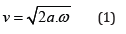
Where ω = 2π/T are the frequencies of temperature changes, T is the oscillation period, p a =κ/cp is the thermal diffusivity coefficient, and κ,cp,ρ are thermal conductivity, specific heat capacity and density of the material, respectively. Thus, the thickness of the anisotropic crystal plate perpendicular to the heat flow d determines the speed of Anisotropic Thermoelectric Detectors [3,4].
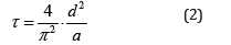
And, accordingly, it sets the cutoff frequency of the transverse thermoelectric voltage generated by them (Figure 1). Since temperature waves are highly attenuated - when exposed to a harmonic heat source they attenuate at a quarter of a wave, they usually degenerate into a temperature front. These slow diffuse waves determine both the large delay in heating and cooling of the Earth and the usually low response speed of thermal detectors. However, due to the high anisotropy of the thermopower of a one-dimensionally incommensurate crystal of higher manganese silicide (HSM) [5], thermal detectors based on the transverse thermoelectric effect (ATE) can operate up to a microsecond, i.e., as can be seen from Figure 1, a cutoff frequency of the order of megahertz is achievable
Figure 1: Amplitudes of the alternating (AC) signal of the Anisotropic Thermoelectric Detector (ATD) depending on the frequency of modulation of the heat flow for different thicknesses of the higher manganese silicide (HSM) plate: points - experiment, lines - calculated curves in accordance with formula 2.

Moreover, in experiments with a one-dimensionally incommensurate HSM crystal nano- modulated along the C axis, both an addition at zero frequency (Figure 1) and a highfrequency addition are observed, which, naturally, cannot be taken into account by formulas 1, 2 of the macroscopic theory. But the detection ability of any thermal detectors is determined, as for any heat engine, by the Carnot cycle and, in principle, is low. In addition, as performance increases, it naturally drops for ADT (Figure 2).
Figure 2:Dependence of the detection ability of thermal detectors on their speed.

Thermo-Electronic Waves in Semiconductor Structures
Studies of contact phenomena [7-10] have shown that giant thermopower arising at contacts, which for a long time was classified as anomalous due to poor reproducibility, become well repeatable if a well-established technology for creating devices based on p-n junctions is used as a working thermal contact (Figure 3).
Figure 3:A p-n junction shielded from radiation by a thin absorbing metal film, brought into thermal contact with a copper radiator..

A series of studies of the EMF of p-n junctions, both when applying a heat flux using close contact, and due to the absorption of radiation in a micron metal film covering the heated plate, gave not only their high reproducibility [11-17], but also made it possible to understand the nature giant Thermo-EMF p-n junctions arising due to Prigogine’s Local Entropy Production [18-23].
The high, three orders of magnitude greater than the diffusion Seebeck coefficient, value of Local Thermo-EMF p-n junctions and their high efficiency of DIRECT, as opposed to INDIRECT- diffuse, conversion of thermal energy lead to the fact that Local Thermo- EMF must be taken into account for the correct description of all Electronics [22-26]. At the same time, near the p-n junction and in structures based on them, the transformation of the temperature wave into a three- component Thermo-Electronic Wave also occurs. In the Thermo-Electronic Wave, due to the heating pulse, in addition to the propagation of Local regions of temperature rise, regions of Local heating, regions of Local Einstein cooling also arise, corresponding to negative temperature half- waves. Thus, the Thermo-Electronic Wave, in contrast to the Electron Wave, which takes into account only electrical and concentration forces, also takes into account the actual temperature force - Local Temperature Gradients (Figure 4). Therefore, with a length of the Thermo-Electronic Wave on the order of the active region of the p-n junction, one could expect that the frequency response of the Local Thermo-EMF would have a resonant character.
Figure 4:Scheme of the appearance when a heating pulse is turned on (left) in a semiconductor structure on a copper n-P-Cu radiator of a spatial distribution of Thermo-Electronic Waves (green line), degenerating over time (lilac curve) into a linear temperature distribution (blue line), determined by the average thermal conductivity of the structure. The movement of the wave front shown in the figure deep into the copper radiator (lilac line) is conditional - for clarity, because Due to the high thermal conductivity of copper, the waves in the massive radiator are attenuated and degenerate into a sharp approach to room temperature (red dotted curve).

Figure 4 Scheme of the appearance when a heating pulse is turned on (left) in a semiconductor structure on a copper n-PCu radiator of a spatial distribution of Thermo-Electronic Waves (green line), degenerating over time (lilac curve) into a linear temperature distribution (blue line), determined by the average thermal conductivity of the structure. The movement of the wave front shown in the figure deep into the copper radiator (lilac line) is conditional - for clarity, because Due to the high thermal conductivity of copper, the waves in the massive radiator are attenuated and degenerate into a sharp approach to room temperature (red dotted curve).
In this case, as shown in Figure 4, when the heating pulse is turned on, the temperature on the surface of the semiconductor structure sharply (with the rate of heating of the thin metal layer) increases almost to the maximum temperature value determined by the heat flow and thermal resistance of the structure (in Figure 4 it is taken as one). And not just a thermal front propagates deep into the semiconductor structure, but Thermo-Electronic Waves (green curve), creating a large temperature gradient, the passage of which through the p-n junction gives a large EMF.
In accordance with Figure 4, we also have the maximum value of the Local Thermo-EMF when the maximum temperature gradient of the Thermo-Electronic Wave passes through the n-P junction, which, with a regular thermal meander, takes on a stationary form with a phase shift determined by the structural parameters. In the region of linear conversion of heat flow power described in [27], for large periods of the heat flow meander, as can be seen from the oscillograms in Figure 5, at the beginning of the thermal pulse there is a sharp positive voltage pulse and a more diffuse negative pulse at its end (Figure 5, 150Hz - 10dB power attenuation). With an increase in the frequency of the thermal meander, it is clearly seen that even at low powers the leading edge of the voltage pulse is followed by a small voltage drop (Figure 5, 1500Hz - 10dB power attenuation). When the frequency of the thermal meander increases by another order of magnitude at low powers (Figure 5, 15kHz - 10dB power attenuation), the voltage drop at the beginning of the pulse does not occur because during half the period, it does not have time to reach the critical “breakdown” amplitude.
Figure 5:Characteristic oscillograms of the dependence of the degree of filling of the response pulse of Local Thermo-EMF in the p-n junction on the duration of the thermal meander pulse and the level (attenuation in dB) of its power.

With an increase in the power of the thermal meander, in accordance with the saturation of the detector signal described in [27] and its drop until the phase reversal, a significant contribution of the “breakdown” pulse is observed at all frequencies of the meander (Figure 5, 0dB). But, as can be seen from Figure 5, the longer the period, the greater the negative contribution.
Thus, the shape of the observed voltage pulses depends on the total pulse accumulated over time at the charge front. The shown more detailed change in the shape of the response pulse of Local Thermo-EMF depending on the power of the meander at a frequency of 475Hz (Figure 6) is fully consistent with the conclusions made above and explains the result given in [27] about the saturation of the effective amplitude of the response of Local Thermo-EMF.
Figure 6:Characteristic saturation at a frequency of 475Hz of the effective amplitude of the response of Local Thermo-EMF with a subsequent reversal of their sign with increasing power of the thermal meander.

The slower negative pulse is probably due to the fact that when the temperature front reaches the boundary of the semiconductor with the copper contact radiator (purple line in Figure 3), the main temperature drop will occur on the thick semiconductor substrate, which will give an antiphase signal at the back edge of the meander. Although, it is possible that the shape of the response pulse is also affected by a process associated with the low work function of electrons from the metal into the semiconductor.
By changing the duration of the period of the thermal meander, bringing it closer to the characteristic times of the described response pulses of the Local Thermo-EMF p-n junction, we change its degree of filling (Figure 5) and, naturally, the amplitude of the effective signal. At powers of the linear conversion range, the frequency response of the effective signal. changes slightly up to a certain frequency at which the signal increases followed by a decrease, the frequency of which is determined by the pulse duration of the leading and trailing edges (Figure 5 & 6). But, at the same time, a special point appears on the current-voltage characteristic of the p-n junction, causing the voltage of the alternating signal to pass through zero when approaching zero frequency (Figure 7).
Figure 7:Zeroing the response signal of Local Thermo-EMF p-n junction with its negative bias.

This special point, which appears when applying both a constant and modulated heat flow, modifies the current-voltage characteristic at direct current, but does not coincide with the passage of the current-voltage characteristic itself through zero and is a special thermodynamic resonance point, relative to which the current-voltage characteristic turns when the heat flow passes through the p-n junction (Figure 8).
Figure 8:Displacement (“rotation”) of the current-voltage characteristic of the p-n junction due to the temperature difference arising on it at different attenuations of the power of the supplied heat flow.

Thus, at modulation frequencies tending to zero, the generated Local Thermo-EMF at a special point of the current-voltage characteristic gives a strict transition to an antiphase signal. In this case, a transformation of the frequency response of the alternating signal occurs and is, moreover, controlled using a constant bias (Figure 9).
Figure 9:Transformation of the frequency characteristic of the effective amplitude of the response of Local Thermo- EMF of a silicon p-n junction when it is biased by direct current.

But, as shown in Figures 9a & 9b, biasing the pn junction reduces the low-frequency signal to zero, and then, after passing a critical current, reverses its phase and, with a further increase in the bias current, increases the amplitude of the signal at low frequencies. In the high-frequency region, the signal monotonically increases somewhat. In this case, the Thermo-Electronic Wave can be modified by external electrical displacement of the p-n junction in such a way that the frequency response characteristic takes on a resonant form (Figure 10). When biased by a critical current, the frequency response takes the characteristic form of a Gaussian resonance, but from the logarithm of the heat flow modulation frequency.
Figure 10:Frequency characteristic of the amplitude of Local Thermo-EMF at a critical (for a given p-n junction) bias (a small change in the heat flow power in the linearity region does not change the shape of the resonance characteristic).

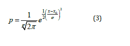
The Resonance shown in Figure 10 has the form of a normal (Gaussian) distribution - probability density: The Gaussian distribution of the random variable X is characterized (in the onedimensional case) by the probability density
The experimentally observed resonance of Local Thermo-EMF at silicon p-n junctions is strictly described by a similar Gaussian, but from the logarithm of frequency (solid line in Figure 10):
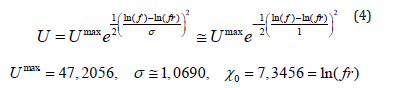
Any component of the velocities of electrons in thermal motion is normally distributed. But the maximums of the distribution of velocities of electrons moving under the influence of the thermal field and the counter flow of electrons moving under the influence of the difference in electrical potentials arising on the layer are separated. In addition, as already noted, we have a contribution to the total flow from the temperature force. And as a result, Thermo- Electronic Oscillation occurs in a ballistic, highly efficient mode. And the fact that the dispersion on a logarithmic scale is equal to unity is very symbolic and is one of the confirmations of the TRUTH of the Principle of Logarithmic Relativity, which manifests itself in IR spectra, and in general for any SCALES, not only energies, but also spatial coordinates, and TIME.
Conclusion
The Principle of Logarithmic Relativity, corresponding to the adiabatic expansion in energy, as noted earlier in [28], manifests itself in the similarity of optical oscillators of different frequency ranges. In this work, Rits.10 clearly demonstrates the manifestation of this Principle within one spectrum over a wide range corresponding to Thermo-Electronic Resonance, arising due to the statistical distribution of several electron flows under the influence of several thermodynamic forces.
References
- Connor JJO, Robertson EF (1997) Jean Baptiste Joseph Fourier, University of St Andrews, Scotland.
- Isachenko VP, Osipova VA, Sukomel AS, Heat Transfer, Third Publishing House, Moscow, Russia, p. 486.
- Anatychuk LI (1979) Thermoelements and thermoelectric devices, Naukova Dumka, Kyiv, Ukraine, p. 766.
- Snarsky AA, Palti AM, Ascheulov AA (1997) Anisotropic thermoelements. Semiconductors 31(11): 1281-1298.
- Ordin SV (2011) In: Optical Lattices: Structures, Atoms and Solitons, “Giant spatial dispersion in the region of plasmon-phonon interaction in one-dimensional- incommensurate crystal the higher silicide of manganese (HSM)”, Benjamin J Fuentes (Ed.), Nova Science Publishers, pp. 101-130.
- Ordin SV (1995) Thermoelectric waves in anisotropic cristal of higher manganese silicide, Proc. XV the Int. Conf. on Thermoelectrics, (ICT'95), St.-Petersburg, Russia, pp. 212-214.
- Ordin SV (1997) Optimization of operating conditions of thermocouples allowing for nonlinearity of temperature distribution. Semiconductors 31(10): 1091-1093.
- Ordin SV (1997) Peltier Heat as a Volume Property and Optimization of Working Regimes of Thermoelements in Real Conditions, Abstracts [PEL-P.2] of the XVI Int. Conf. on Thermoelectrics (ICT'97), Dresden, Germany, pp. 96-97.
- Okamoto Y, Ordin SV, Miyakawa T, Fedorov MI, Miida Y, Miyakawa T (1999) IR-characterization of sintering SiC thermoelectric semiconductors with use of 4-component effective medium model. Journal of Applied Physics 85(9): 6728-6737.
- Ordin SV (2002) Contact Thermopowers, Abstract, Proceedings of ICT'02 XXI International Conference on Thermoelectrics Long Beach, CA, USA.
- Ordin SV, Sokolov IA, Zjuzin AJ (2006) Thermoelectric processes in p-n junctions, Works of X interstate seminar: Thermoelectrics and their application, A.F. Ioffe PhTI of the Russian Academy of Sciences, St.-Petersburg, Russia, pp. 41- 47
- Ordin SV, Wang WN (2008) Thermoelectric properties nano structures, PH-TI of A.F. Ioffe of the Russian Academy of Sciences, St.-Petersburg, Russia Works of XI interstate seminar: Thermoelectrics and their application, pp. 55-60
- Ordin SV, Zjuzin A Yu, Ivanov Yu, Yamaguchi S (2009) Nano-structured materials for thermoelectric devices, NATO Workshop "Advanced Materials and Technologies for Micro/Nano-Devices, Sensors and Actuators", St Petersburg, Russia.
- Ordin SV, Zjuzin AJ, Yu Ivanov, Yamaguchi S (2010) Nano-structured materials for thermoelectric devices, The 29th International Conference on Thermoelectrics, Shanghai, China, p. 1-14.
- Ordin SV, Wang WN (2011) Thermoelectric Effects on Micro and Nano Level. J Advances in Energy Research 9: 311-342.
- Ordin SV, Yu V Zhilyaev, Zelenin VV, Panteleev VN (2017) Local thermoelectric effects in wide-gap Semiconductors. Semiconductors 51(7): 883-886.
- Ordin SV (2017) Refinement and Supplement of Phenomenology of Thermoelectricity. American Journal of Modern Physics 6(5): 96-107.
- Ordin SV (2017) Cardinal increase in the efficiency of energy conversion based on local thermoelectric effects. International Journal of Advanced Research in Physical Science 4(12): 5-9.
- Ordin SV (2018) Experimental and theoretical expansion of the phenomenology of thermoelectricity. Global Journal of Science Frontier Research- Physics & Space Science (GJSFR-A) 18(1): 1-8.
- Ordin SV (2018) Cardinal increase in the efficiency of energy conversion based on local thermoelectric effects. J Mater Eng Appl (JMEA) 1(1): 17-20.
- SV Ordin (2018) Anomalies in thermoelectricity and reality are local thermo-EMFs. Journal of Materials Engineering and Applications.
- SV Ordin, Mistakes in the theory of p-n junction and fundamentals of thermophotoelectronics. World Journal of Condensed Matter Physics (WJCMP).
- SV Ordin (2023) Foundations of Thermoelectronics. International Journal of Physics and Mathematics. IJPM 5(1): 15-19.
- SV Ordin (2023) Introduction to thermo-photo-electronics. Journal of Electronic & Information Systems 5(1): 51-66.
- SV Ordin (2023) Ballistic thermoelectricity. International Journal, Advanced Energy Conversion Materials 4(2):139-146.
- SV Ordin, Sharrupin BN (1998) Normal lattice oscillations and crystalline structure of non-isotropic modifications of a boron nitride. J Semiconductors (FTP) 32(9): 924-932.
- Okamoto Y, Ordin SV, Miyakawa T (1999) IR-characterization of sintering SiC termoelectric semiconductors with use of 4-component effective medium model. Journal of Applied Physics 85(9): 6728-6737.
- Ordin SV, Shelykh AI (2010) Optical and dielectric properties of rare-earth oxide Lu2O3. J Physics and Technics of Semiconductors 44: 558-563.
© 2023 Stanislav Ordin. This is an open access article distributed under the terms of the Creative Commons Attribution License , which permits unrestricted use, distribution, and build upon your work non-commercially.
Editor In Chief


.jpg)


Signup for Newsletter

Quick Links
 Editorial Board Registrations
 Submit your Article
 Refer a Friend
 Advertise With Us
Our Recent Edition

.jpg)


Top Editors


.jpg)


.bmp)
.jpg)
.png)
.jpg)


.jpg)


.png)

.png)


.png)


Financial Support

Sponsors

Latest e-Books

Latest Video

 a Creative Commons Attribution 4.0 International License. Based on a work at www.crimsonpublishers.com.
Best viewed in
a Creative Commons Attribution 4.0 International License. Based on a work at www.crimsonpublishers.com.
Best viewed in