- Submissions

Full Text
Trends in Textile Engineering & Fashion Technology
Surface Roughness and Seeding Process Influence on Boron Doped Micro/Nanocrystalline Diamond Adhesion on Titanium Substrate
Marta Santos1,2, Silvia S Oishi2* and Neidenei G Ferreira2
1 Faculty of Technology of the State of São Paulo (Fatec), Brazil
2 LAS, National Institute for Space Research (INPE), Brazil
*Corresponding author: Silvia S Oishi, LAS, Instituto Nacional de Pesquisas Espaciais (INPE), Av. dos Astronautas 1758, São José dos Campos-SP, CEP 12227-010, Brazil.
Submission: November 21, 2018;Published: December 04, 2018

ISSN 2578-0271 Volume4 Issue5
Abstract
CVD (Chemical Vapor Deposition) diamond deposition on different materials requires surface treatment such as diamond particles seeding on the substrate dispersed in an appropriate solvent by using ultrasonic agitation. On the other hand, seeding process by electrostatic attraction of nanodiamond particle have produced films with higher nucleation density compared to that obtained from ultrasonic treatment. In addition, nucleation and growth of micro/nanocrystalline boron doped diamond films (BDD/NBDD) on titanium (Ti) substrates represent a complex process, mainly due to the poor film adhesion related to the difference in the thermal expansion coefficients between the film and the substrate. Thus, the substrate morphology associated to the seeding process can be determinant for this adhesion. In this context, the adhesion of BDD and NBDD films on Ti substrate was systematically considered in five different Ti surface roughness associated to two different seeding processes: ultrasonic agitation with 0.25μm diamond particle and electrostatic seeding with 4nm diamond particle in potassium chloride. Thus, twenty different diamond film sample sets were grown by CVD technique following the combinations of BDD and NBDD morphologies, Ti roughnesses, and seeding methodologies. The samples were characterized by scanning electron microscopy, Raman scattering spectroscopy, and X-ray diffraction (XRD). The adhesion tests were performed by the Rockweel hardness test according to VDI 3198. The results showed that the BDD and NBDD films grown with electrostatic seeding with 4nm diamond particle presented the best adhesion regardless of substrate roughness while only the Ti substrates with higher roughness presented good adhesion for ultrasonic agitation pre-treatment with 0.25μm diamond particle. These results indicate that the electrostatic seeding pre-treatment associated with greater surface roughness have an important role in improving diamond films adhesion for the two studied morphologies.
Keywords: Micro/nanocrystalline boron doped diamond; HFCVD; Diamond seeding; Titanium; Adhesion
Introduction
CVD (Chemical Vapor Deposition) diamond deposition on titanium (Ti) substrate is a way to promote a significant improvement for industrial applications especially as electrodes since Ti present corrosion and mechanical stability in addition to the good electrochemical properties of boron doped diamond (BDD) [1,2]. Different authors have been studying diamond adhesion on Ti as well as the Ti surface pretreatment using different processes [1,3,4]. The manual substrate scratching or abrasion by different diamond powders can increase the diamond nucleation rate [5]. One of the most widely used approaches is the substrate seeding with diamond particles dispersed in an appropriate solvent accompanied by ultrasonic agitation [6,7]. Other widely used method in the scientific and the more efficient the BEN (from English Bias Enhanced Nucleation. The process consists in applying a difference of potential between the substrate and the activation region. With this potential difference, the ions are accelerated toward the substrate promoting an increase in nucleation density [8]. This is one of the most efficient processes reported in the literature, since the nucleation rate is from 108 up to 1011cm-2.
A process as efficient as BEN, but without the inconvenient incorporation of graphite particles in the film, is the process of seeding with 4nm diamond particles on the substrate. This process consists in saturate the surface of the substrate with nanometric diamond, before the process of growth and, thus, to obtain a high nucleation density [9]. Depending on the treatment, the nucleation rates can reach densities of the order of 1011cm-2. For the electrostatic interaction between diamond nanoparticles and substrate, Kim et al. [10] have discussed the process called the ESAND (Electrostatic Self-assembly Seeding of Nanocrystalline Diamond), in which the substrate surface energy was modified from functionalization with a polymer soluble in water or in another solvent [10]. This technique allowed them to produce a polycrystalline diamond onto an oxide film without mechanical damage.
Besides the seeding process, the substrate roughness also represents a significant contribution on diamond film adhesion that can be favorable on its anchorage course. Mallik et al. [11] have discussed the substrate roughness influence on diamond growth on silicon substrate. They concluded that the substrate roughness has a strong effect on the morphology and quality of diamond coatings grown on Si (100) substrate by hot filament CVD technique. As the depth of valley increases with surface roughness, more diamond particles get embedded within the asperities and through of the surface enhancing diamond nucleation in addition to improve its growth behavior. Lim et al. [1] have also studied the stability of Ti-based BDD (boron doped diamond) electrode involving the surface roughening. They showed that a roughened substrate surface is essential to reduce the thermal stress built-up in the BDD film grown on the Ti substrate and, consequently, improving the diamond film adhesion.
Taking in mind the above information, a systematic study was performed concerning the adhesion of BDD and NBDD (nanocrystalline boron doped diamond) films on Ti substrate. Five different Ti surface roughness were considered for two different seeding processes: ultrasonic agitation with 0.25μm diamond particle and electrostatic seeding with 4nm diamond particle in potassium chloride. Twenty different diamond film samples were grown by CVD technique for 20h, allowing for the combination of BDD and NBDD morphologies, Ti roughness, and seeding methodologies. The samples were characterized by scanning electron microscopy, Raman scattering spectroscopy, X-ray diffraction (XRD), and optical profilometry. The adhesion tests were performed by the Rockweel hardness test according to VDI 3198 [12].
Experimental
BDD and NBDD were grown on Ti substrates (surface area of 1.0 x 1.0cm2) by Hot Filament Chemical Vapor Deposition (HFCVD) technique. Diamond deposition on titanium has a singular characteristic attributed to the strong stress formation between the film and the substrate, which arises from extrinsic and intrinsic factors, but is mainly attributed to the large thermal coefficient mismatch between them. In this sense, some pre-treatments on the substrate surface are required to decrease the stress as well as to increase the nucleation rate. Five types of differently treated Ti-substrates were used for diamond deposition, following their roughness decrease as: sandblasted to provide a rough surface relief (SB), as-received (AS), polished with sandpaper 80 (SP80), polished with sandpaper 600 (SP600), and polished with sandpaper 2000 (SP2000). All the treated Ti-substrates were submitted to the two different seeding processes: ultrasonic agitation with 0.25μm diamond particle, named US, and electrostatic seeding with 4nm diamond particle in potassium chloride, named ES. For the US process, the substrate is ultrasonically abraded in a suspension containing 0.25μm diamond powder in hexane for 1h. For the ES process, firstly, the substrates were chemically attacked with ammonium fluoride 40% solution for about 2s to remove the native oxide layer. Secondly, they were submitted to surface modification by dipping it in a solution with 10wt% of the cationic polymer Poly Diallyl Dimethyl Ammonium Chloride (PDDA) for 30 min, quickly immersed in DI water, and dried with nitrogen gas flow. Finally, they were immersed in colloidal solution of 1mM KCl + 4nm (ND particles) for 10 min [13].
Then, twenty different diamond film samples sets were produced and characterized, following the combinations of BDD and NBDD morphologies, Ti roughness, and seeding methodologies. The HFCVD set up allowed to produce six samples in the same experimental condition for each growth process. For BDD films the gas mixture was 198:2 sccm of H2:CH4 while the NBDD was grown with 184:16 sccm of H2:CH4. The boron source was obtained from a constant flow of 30 sccm for an additional H2 line passing through a bubbler containing the B2O3 dissolved in methanol with B/C ratio 30000ppm. Thus, the boron was carried from the solution to the gas phase by this H2 line where its additional flux in the reactor was controlled by a rotameter. This boron content was used for both BDD and NBDD morphologies. The adherence study was performed by using well-known Rockwell C indentation test with using a Hardness tester with diamond tip cone shape 120°, model 20-70 HRC/HR-150A applying a initial load of 10kgf followed a second load of 50kgf, as prescribed by the VDI 3198 norm [12]. All films were grown for 20h, at 650°C by controlling the pressure of 30 Torr inside the reactor chamber. Top view FEG-SEM images of substrates as well as of micro/nano diamond films were obtained from a Tescan Mira 3. The diamond quality was analyzed by Micro- Raman spectra recorded using a 514.5nm line of argon ion laser, LabRAM HR evolution equipment from Horiba Scientific. The diamond patterns in addition to hydrides and titanium carbides phases were monitored using a PAN analytical model X’Pert PRO MPD diffractometer with the CuK α radiation (λ=1.54 Å). Ti and BDD/NBDD surface roughness were evaluated by profilometry technique using a Veeco WYKO NT 1100 system.
Results and Discussions
SEM analyses
Concerning Ti substrates, it is important to point out that the mechanical polishing of titanium is not an easy process because titanium is a very ductile material and because of this, its polishing process can lead to material deformation and detachment, which may become impregnated on the sandpaper surface and/or on the used polishing powder. Figure 1 shows SEM images from (a) to (e) related to the five types of differently treated Ti-substrates that were used for diamond deposition, following their roughness decrease as: sandblasted to provide a rough surface relief (SB), as-received (AS), polished with sandpaper 80 (SP80), polished with sandpaper 600 (SP600), and polished with sandpaper 2000 (SP2000). For the SB samples, the mechanical incision is effective to increase the titanium surface area and roughness besides improving the film mechanical anchoring. This roughness is significant, since in this magnification, different depths can be observed, considering the top surface compared to hole depths. The AS sample (Figure 1(b)) also presents homogeneous and welldefined hole distributions, but with lower roughness than that of SB surface. For the samples treated with sandpaper of different grades, the morphology certainly changed, passing to a more uniform roughness which decreases as the sandpaper grades increase, as expected. Nonetheless, for Figure 1(c), the scratches of SP80 are well evident while for Figure 1(d) residual material from polishing process can be detected as the small particles over the sample surfaces related to the SP granulometry. On the other hand, the sample SP2000 presents a well polished and almost mirrored surface to the naked eye.
Figure 1:SEM images of Ti substrates: (a) SB, (b) AS, (c) SP80, (d) SP600, and (e) SP2000.
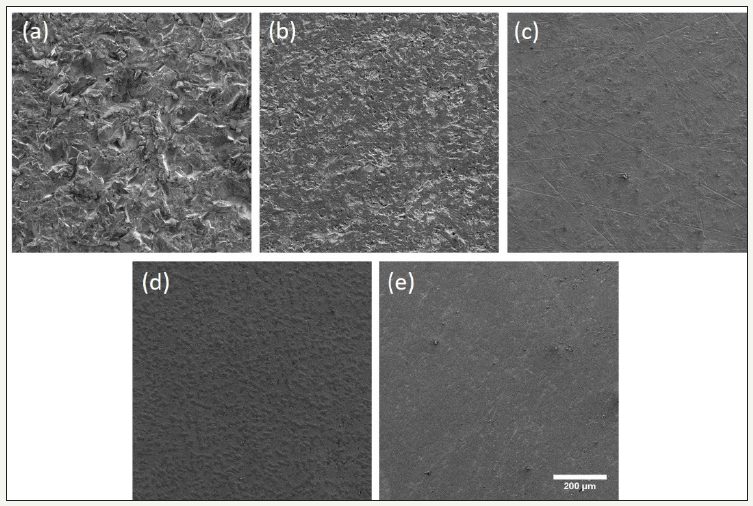
Figure 2:FEG-SEM images of samples (a) BDD/SBTi and (b) BDD/SP2000Ti for US pre-treatment while (c) BDD/SBTi and (d) BDD/ SP2000Ti for ES pre-treatment
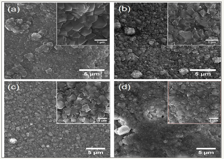
Top view SEM images are discussed for BDD and NBDD samples taking into account their highest and lowest Ti roughness for both seeding methodologies. Thus, Figure 2 shows the BDD film morphologies for both US (ultrasonic agitation) and ES (electrostatic seeding) Ti pre-treatments, where samples (a) and (b) refer to the BDD/SBTi and BDD/SP2000Ti for US pre-treatment while samples (c) and (d) are related to BDD/SBTi and BDD/SP2000Ti for ES pretreatment. For a better visualization of the grain morphologies, their respective insets are in higher magnifications. All the images show continuous and homogeneous films covering the entire substrates. Considering the challenge to grow diamond on Ti, the films did not present cracks or delaminations. This result is important because the diamond growth on Ti substrates presents two problems. The first concerns the difference of the thermal expansion coefficients between Ti and diamond. The second may be related to the formation of intermediate phases such as hydrides and titanium carbides, which depend on the substrate pre-treatment, the carbon source content on the gas phase, and the substrate temperature [14]. The BDD morphology is associated to the microcrystalline grains randomly oriented.
Some studies published in the literature dealing with the diamond deposition on titanium substrates have linked the cauliflower-like formed microstructures to the microcrystalline grain agglomerates [14,15]. The morphology behavior was similar for this sample set regardless of the Ti roughness even by comparing the grain size, better evidenced in the Figure 2(a,b) insets, which did not show a significant difference. Nonetheless, when the electrostatic seeding with 4nm diamond particle was used, for both Ti substrate roughness, the diamond grain size decreased (Figure 2(c,d) insets), more evident for BDD/SP2000Ti sample. This behavior is related to the initial stages of film growth, when the 4nm diamond seeds were used. For this methodology, the diamond nucleation density is expected to be higher than that for seeding with diamond powder of 0.25μm. Therefore, before the steady state to be established, for the known diamond columnar growth, the high nucleation rate promoted by the ES pre-treatment certainly assured the grain competition on the growth surface primarily favored by the lowest surface roughness. That means the smoothest SP2000Ti surface avoided the clusters formation by the 4nm diamond powder.
Following the same format, the images for NBDD films are shown in Figure 3 where samples (a) and (b) refer to NBDD/ SBTi and NBDD/SP2000Ti for US pre-treatment while samples (c) and (d) are related to NBDD/SBTi and NBDD/SP2000Ti for ES pre-treatment. Their image insets are in higher magnifications. The surfaces consist of ball-like diamond particles, which present a relatively wide distribution of sizes and morphologies. For US seeding, the nucleation mechanism is similar to that of abrasion process in which the embedded diamond fragments help the nucleation of sp3 diamond phase, while the density of diamond seeds is also related to the concentration of diamond suspension and to the size of dispersed diamond powder. On the other hand, for ES the interaction of nanodiamond particles occurs according to the ESA (Electrostatic Self-Assembly) method, based on a multilayer construction by electrostatic attraction between opposite charges on each layer. Thus, the later supply an extremely high nucleation density (>1011 cm-2) and homogeneous surface because the functionalization process allows a called nanodiamond seeding [16]. Also, it is important to point out that CH4 in the precursor mixture has a profound effect on the morphology and properties of the diamond coatings. The nucleation density, nucleation rate, and adhesion strength of the diamond coatings can be enhanced by increasing the CH4 concentration [17]. In this sense, the NBDD were grown with high CH4 concentration in the gas mixture, around 8% which caused the expected secondary nucleation of these morphologies.
Figure 3:FEG-SEM images of samples (a) BDD/SBTi and (b) BDD/SP2000Ti for US pre-treatment while (c) BDD/SBTi and (d) BDD/ SP2000Ti for ES pre-treatment

Optical profilometry
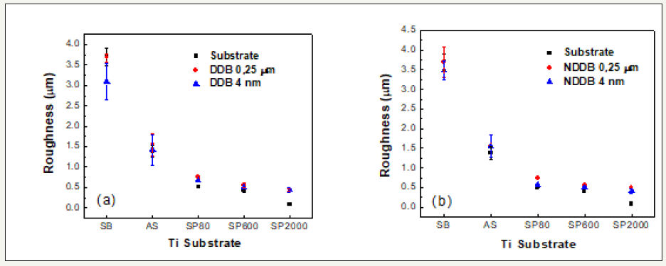
Figure 4 shows the results of average surface roughness (Ra) obtained by optical profilometry, in five different points, for all Ti substrates considering the two pre-treatments studied (US and ES), before and after both BDD and NBDD growths. The substrate roughnesses are well correlated with SEM images which show from higher roughness of SB surface to lower roughness after polishing AS substrate with different sandpaper grades. Figure 4(a) shows surface roughness for BDD films with US and ES pre-treatments. In general, diamond growth follows the substrate morphology, but it is possible to notice for BDD/SBTi a decrease in surface roughness when ES pre-treatment is used. This is probably related to the higher nucleation density provided by this seeding treatment that fills small pits. For the other substrates AS, SP80, SP600, and SP2000, BDD films roughness becomes dominant and induces a slight increase in comparison to their respective substrate roughness. Usually nanocrystalline diamond surface is smoother than that of microcrystalline morphology nevertheless, Figure 4(b) shows a similar behavior for NBDD with approximated values to those of BDD surface roughness. The roughness decreased only for samples obtained from ES of 4nm diamond powder comparing to those obtained from US of 0.25μm, showing that the substrate seeding process also promoted great influence on NBDD film roughness.
Figure 4:Average roughness profile of (a) BDD and (b) NBDD films grown on different substrate roughness with US and ES pretreatment.
Raman analyses
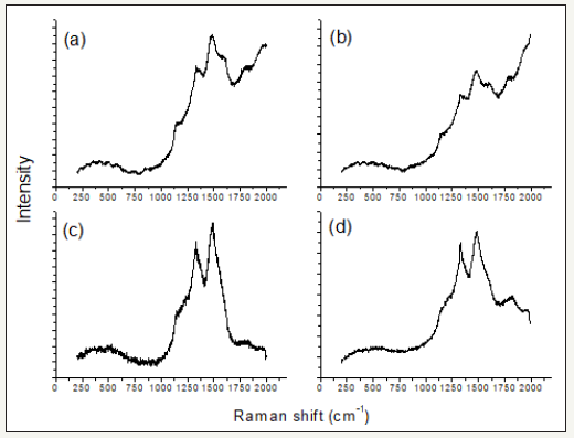
The quality of BDD and NBDD films investigated by Raman spectroscopy is shown in Figure 5&6, respectively, using the same format for data presentation where the film spectra were grouped taking into account the ordering for the spectra: (a) and (b) for US pre-treatment while (c) and (d) represent the samples for ES pre-treatment. Figure 5 related to BDD spectra depicts the presence of the following characteristics bands: the diamond peak around 1332cm-1, the band at 1230cm-1 characteristic of boron doping, and the band around 500cm-1 related to an increase in the concentration of boron pairs [18-20]. In our BDD Raman spectra, the peak at 1480cm-1 assigned to transpolyacetylene and the G band at around 1590cm-1 attributed to graphitic phases are also present. These bands indicate that non-diamond bound carbons are present, mainly in the nucleation film layer possibly due to the low temperature of diamond growth [21]. From the spectra of Figure 5(a,b) no significant differences are observed associated to the substrate roughness. Nevertheless, by comparing the spectra of Figure 5 (a,c) or Figure 5(b,d) we can infer that the ES pre-treatment, associated to 4nm diamond powder, exhibits a more pronounced band at around 1480cm-1, confirming a high nucleation rate promoted by ES pre-treatment associated to transpolyacetylene incorporation increase in these films. This behavior is in accordance with SEM images (c) and (d) of Figure 2, where a diamond grain size decrease was observed leading to an increase in diamond grain boundary density, naturally causing nondiamond carbon arise. In addition, from this comparison, it appears that the 500 and 1230cm-1 bands on spectrum of Figure 5(c) are less pronounced than those of spectrum (a) indicating an apparent doping decrease. This behavior suggests that boron incorporation followed an alternative pathway to the sp2 bonds.
Figure 5:Raman spectra of samples (a) BDD/SBTi and (b) BDD/SP2000Ti for US pre-treatment while (c) BDD/SBTi and (d) BDD/ SP2000Ti for ES pre-treatment.
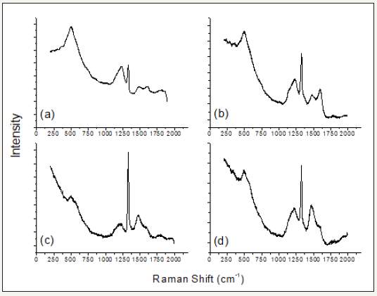
Figure 6 presents the Raman spectra for the sample set of NBDD films. For all spectra, the diamond peak is hindered by D band, as expected for nanocrystalline (NCD) films, considering the Raman excitation with visible laser of 514nm. Both D and G bands are attributed to sp2 carbon presence. The TPA peaks at 1150 and 1470 cm-1 also appear and can be considered as a fingerprint of nano and ultrananocrystalline diamond [22]. The boron doping bands at 500 and 1220cm-1 can be viewed with less prominence.
Figure 6:Raman spectra of samples (a) NBDD/SBTi and (b) NBDD/SP2000Ti for US pre-treatment while (c) NBDD/SBTi and (d ) NBDD/SP2000Ti for ES pre-treatment.
For BDD or NBDD films the Raman features were similar to those discussed above for samples grown on AS/Ti, SP80/Ti, and SP600/Ti after the two pre-treatments (not shown).
XRD analyses
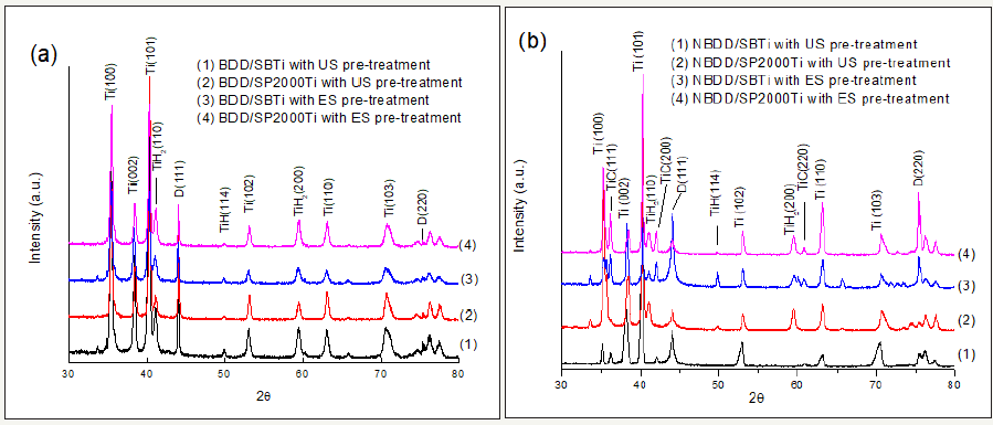
The phase composition and crystal structure are characterized by XRD shown in Figure 7(a,b) for BDD and NBDD films, respectively. For all sample sets studied the diamond diffraction planes are clearly depict at 2θ = 44° and 75.5°, corresponding to the (111) and (220) planes, respectively. The XRD patterns also show the formation of Ti planes (100), (002), (101), (110) and (103), TiH plane (114), and TiH2 plane (110) and (200) of BDD and NBDD films [23,24]. Three peaks related to the TiC phase (111), (200), and (220) are well evident for all NBDD samples grown with ES pre-treatment, but only for NBDD/SBTi when US pre-treatment is used. This TiC formation is important to avoid the Ti hydrogenation process that may be related to the cracking progress in diamond film.
For BDD films (Figure 7(a)), the comparison between (111) and (220) peak intensities indicates that the films have preferred orientation with (111) facet. Considering this concentration of CH4(~1%), it is expected the TiH phase formation as observed in the patterns of Figure 7(a). For NBDD films, some differences in XRD patterns may be expected since by increasing the methane concentration, the nucleation density as well as the film thickness increase preventing the hydrogen diffusion throughout the Ti substrate [24]. A higher CH4 amount in the gas phase also contributed to the secondary nucleation process of nanocrystalline grains. This is reflected in the intensity increase of (220) diamond diffraction plane mainly for samples obtained from ES pre-treatment of Figure 7(b).
Figure 7:XRD patterns of (a) BDD/SBTi and BDD/SP2000Ti, (b) NBDD/SBTi and NBDD/SP2000Ti samples with different seeding pretreatment.
Indentation test and film adherence
Figure 8:FEG-SEM images of: (a) and (b) BDD/SBTi, (c) and (d) BDD/ASTi, (e) and (f) BDD/SP80Ti, (g) and (h) BDD/ SP600Ti, and (i) and (j) BDD/SP2000Ti. The left column refers to samples with US pre-treatment and the right column are samples with ES pre-treatment.
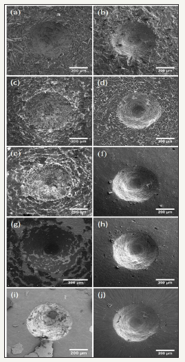
The Rockwell C hardness test method is a qualitative technique to evaluate the adhesion characteristics of the coatings. This test is prescribed by the VDI 3198 norm as a destructive quality test for coated compounds [12], inducing massive plastic deformation to the substrate and a coating fracture. For this study the two complete sample set images are shown in Figure 8&9 for BDD and NBDD, respectively, after Rockwell C indentation for both seeding pre-treatments. The BDD samples produced from US pre-treatment presented the delamination increase as the Ti surface roughness decrease, where the substrate mechanical anchoring is dominant for the film adhesion. Particularly from the image (E), BDD/SP80Ti (0.25μm) the film delamination becomes clear with the Ti plastic deformation. On BDD/SP2000Ti (0.25μm) sample after indentation a severe spallation of diamond coating around the indenter imprint occurred, indicating a very weak interfacial film/substrate bonding. This spallation did not take place for BDD samples produced from ES 4nm pre-treatment even for the smoothest Ti surface (BDD/SP2000Ti). This sample presents only fine radial film cracks, but not yet a delamination process. One determinant factor for this behavior may be associated to the rapid nucleation density from ES methodology that can effectively increase the contact area of diamond coating and Ti substrate, mainly prevent the Ti hydrogenation. For the NBDD films, the adhesion results were similar although some works have demonstrated superior adhesion of microcrystalline diamond (MCD) in comparison to that of nanocrystalline diamond (NCD) grown on WC-Co substrate owing to the presence of non-diamond phases and low hardness of NCD [25,26]. However, the use of Ti as substrate can improve NCD adhesion in the case of diamond deposition under high CH4 concentration. The abundant carbon source supply may promote a simultaneous formation of TiC that acts as a diffusion barrier preventing carbon and hydrogen penetration into Ti substrate in addition to reducing thermal stress [27]. Also, Fu et al. [23] observed that smaller grain sizes led to a better performance in adhesion strength using Ti substrate. According to Askari [28], the use of a moderate temperature for diamond deposition on Ti can decrease the diffusion coefficient of carbon in Ti enhancing the nucleation density and the interfacial adhesion.
Figure 9:FEG-SEM images of: (a) and (b) NBDD/SBTi, (c) and (d) NBDD/ASTi, (e) and (f) NBDD/SP80Ti, (g) and (h) NBDD/ SP600Ti, and (i) and (j) NBDD/SP2000Ti. The left column refers to samples with US pre-treatment and the right column are samples with ES pre-treatment.

Conclusion
A comparative study between the adhesion of boron doped micro and nanocrystalline diamond was conducted using five different Ti surface roughnesses and two seeding pre-treatments. The use of electrostatic seeding with 4nm diamond particle resulted in greater adhesions for BDD and NBDD regardless of substrate roughness that is probably related to the fastest nucleation density promoted by this seeding. The substrate roughness also contributed to improve the adhesion as the sandblasted and as-received samples did not present delamination when both seeding pre-treatments were used. On the other hand, a large detachment was observed for the substrates polished with sandpaper when ultrasonic agitation with 0.25μm diamond particle was used to grow BDD or NBDD. Therefore, the use of ES pre-treatment associated with greater roughness of Ti substrate can significantly improve BDD and NBDD film adhesions.
Acknowledgement
The authors acknowledge CAPES, São Paulo Research Foundation (FAPESP) grant number 2016/13393-9 and Fatec Pindamonhangaba (Centro Paula Souza).
References
- Lim PY, Lin FY, Shih HC, Ralchenko VG, Varnin VP, et al. (2008) Improved stability of titanium based boron-doped chemical vapor deposited diamond thin-film electrode by modifying titanium substrate surface. Thin Solid Films 516(18): 6125-6132.
- Gerger I, Haubner R, Kronberger H, Fafilek G (2004) Investigation of diamond coatings on titanium substrates for electrochemical applications. Diam Relat Mater 13(4-8): 1062-1069.
- Li C, Dai W, Li M, Li H, Xu S, et al. (2016) Effect of sputtered titanium interlayers on the properties of nanocrystalline diamond films. J Appl Phys 119, doi:10.1063/1.4945577.
- Braga NA, Baldan MR, Ferreira NG (2012) From micro to nanocrystalline diamond grown on 3D porous titanium matrix. J Mater Sci 47(1): 23-40.
- Buijnsters JG, Celis JP, Hendrikx RWA, Vázquez L (2013) Metallic seed nanolayers for enhanced nucleation of nanocrystalline diamond thin films. J Phys Chem C 117(44): 23322-23332.
- Williams OA, Douhéret O, Daenen M, Haenen K, Osawa E, et al. (2007) Enhanced diamond nucleation on monodispersed nanocrystalline diamond. Chem Phys Lett 445(4-6): 255-258.
- Buijnsters JG, Vázquez L, Ter Meulen JJ (2009) Substrate pre-treatment by ultrasonication with diamond powder mixtures for nucleation enhancement in diamond film growth. Diam Relat Mater 18(10): 1239- 1246.
- Janischowsky K, Ebert W, Kohn E (2003) Bias enhanced nucleation of diamond on silicon (100) in a HFCVD system. Diam Relat Mater 12(3-7): 336-339.
- Daenen M, Williams OA, D’Haen J, Haenen K, Nesládek M (2006) Seeding, growth and characterization of nanocrystalline diamond films on various substrates. Phys Status Solidi 203: 3005-3010.
- Kim JH, Lee SK, Kwon OM, Hong SI, Lim DS (2009) Thickness controlled and smooth polycrystalline CVD diamond film deposition on SiO2 with electrostatic self-assembly seeding process. Diam Relat Mater 18(10): 1218-1222.
- Mallik AK, Binu SR, Satapathy LN, Narayana C, Seikh MM, et al. (2010) Effect of substrate roughness on growth of diamond by hot filament CVD. Bull Mater Sci 33(3): 251-255.
- Vidakis N, Antoniadis A, Bilalis N (2003) The VDI 3198 indentation test evaluation of a reliable qualitative control for layered compounds. J Mater Process Technol 143-144: 481-485.
- Liu X, Yu T, Wei Q, Yu Z, Xu X (2012) Enhanced diamond nucleation on copper substrates by employing an electrostatic self-assembly seeding process with modified nanodiamond particles. Colloids Surfaces A Physicochem Eng Asp 412: 82-89.
- Braga NA, Cairo CCA, Almeida EC, Baldan MR, Ferreira NG (2009) Temperature influence on the interlayer and surface morphology of diamond coating on 3D porous titanium substrates. Diam Relat Mater 18(9): 1065-1069.
- Buccioni E, Braca E, Kenny JM, Terranova ML (1999) Processingstructure- adhesion relationship in CVD diamond films on titanium substrates. Diam Relat Mater 8(1): 17-24.
- Yoshikawa T, Reusch M, Zuerbig V, Cimalla V, Lee KH, et al. (2016) Electrostatic self-assembly of diamond nanoparticles onto al- and n-polar sputtered aluminum nitride surfaces. Nanomaterials 6(11): 217.
- Wang M, Chu PK (2016) Nanocrystalline diamond coatings. Encycl Plasma Technol, CRC Press, USA, pp. 857-873.
- Ager JW, Walukiewicz W, McCluskey M, Plano MA, Landstrass MI (1995) Fano interference of the Raman phonon in heavily boron-doped diamond films grown by chemical vapor deposition. Appl Phys Lett 66: 616.
- Zhang RJ, Lee ST, Lam YW (1996) Characterization of heavily borondoped diamond films. Diam Relat Mater 5(11): 1288-1294.
- May PW, Ludlow WJ, Hannaway M, Heard PJ, Smith JA, et al. (2008) Raman and conductivity studies of boron-doped microcrystalline diamond, facetted nanocrystalline diamond and cauliflower diamond films. Diam Relat Mater 17(2): 105-117.
- Rath P, Khasminskaya S, Nebel C, Wild C, Pernice WHP (2013) Diamondintegrated optomechanical circuits. Nat Commun 4: 1-9.
- Kulisch W, Petkov C, Petkov E, Popov C, Gibson PN, et al. (2012) Low temperature growth of nanocrystalline and ultrananocrystalline diamond films: A comparison. Phys Status Solidi 209: 1664-1674.
- Fu Y, Yan B, Loh N, Sun C, Hing P (1999) Deposition of diamond coating on pure titanium using micro-wave plasma assisted chemical vapor deposition. J Mater Sci 34(10): 2269-2283.
- Migliorini FL, Alegre MD, Baldan MR, Lanza MRV, Ferreira NG (2014) Doped diamond electrodes on titanium substrates with controlled sp2/ sp3 hybridization at different boron levels. Thin Solid Films 564: 97-103.
- Dumpala R, Kumar N, Kumaran CR, Dash S, Ramamoorthy B, et al. (2014) Adhesion characteristics of nano- and micro-crystalline diamond coatings: Raman stress mapping of the scratch tracks. Diam Relat Mater 44: 71-77.
- Zhang J, Wang X, Shen B, Sun F (2014) Effect of deposition parameters on micro- and nano-crystalline diamond films growth on WC-Co substrates by HFCVD. Trans Nonferrous Met Soc China 24(10): 3181-3188.
- Li YS, Yang L, Tang Y, Zhang C, Zhang L, et al. (2011) Adherent nanocrystalline diamond coatings deposited on Ti substrate at moderate temperatures. Surf Coatings Technol 206(7): 1971-1976.
- Jawid AS, Lu F (2008) Characteristics of a well-adherent nanocrystalline diamond thin film grown on titanium in Ar/CH4 microwave CVD plasma. Vacuum 82(6): 673-677.
© 2018 Silvia S Oishi . This is an open access article distributed under the terms of the Creative Commons Attribution License , which permits unrestricted use, distribution, and build upon your work non-commercially.
 a Creative Commons Attribution 4.0 International License. Based on a work at www.crimsonpublishers.com.
Best viewed in


.jpg)


 Editorial Board Registrations
 Submit your Article
 Refer a Friend
 Advertise With Us
.jpg)


.jpg)


.bmp)
.jpg)
.png)
.jpg)


.jpg)


.png)

.png)


.png)


