
- About Us
- Information
-

The Author ensures that the research has been conducted responsibly and ethically with adherence to all relevant regulations. read more..
- For Authors
- For Reviewer
- Manuscript Guidelines
- Membership
- Publication Ethics
-
- Journals
- Reprints
- e-Books
- Videos
- Policies
- Contact Us
 COVID-19
- Submissions


Full Text
Research & Development in Material Science
Plasmonic Refractive Index Sensor Using Two Cavity Resonators for Sensing Applications
Javad Ostadieh1 and Mir Hamid Rezaei2*
1Department of Electrical Engineering, Khoy Branch, Islamic Azad University, Khoy, Iran
2Department of Communications and Electronics, School of Electrical and Computer Engineering, Shiraz University, Iran
*Corresponding author:Mir Hamid Rezaei, Department of Communications and Electronics, School of Electrical and Computer Engineering, Shiraz University, Shiraz, Iran
Submission: July 24, 2023;Published: August 10, 2023

ISSN: 2576-8840 Volume 19 Issue 2
Abstract
In this paper, a plasmonic refractive index sensor for sensing applications in the near-infrared region is presented. The sensor is composed of two straight waveguides and two square-shaped cavities to utilize the resonance effect. The waveguides and cavities are created by pattering a silver substrate. The effect of geometrical parameters and refractive index changes on the reflection spectrum and sensitivity of the sensor are investigated. Simulations are performed using the finite-difference time-domain method. Simulation results show that the sensitivity of the device reached 1670nm/RIU. Additionally, the total footprint of the device is 1.5μm2. The high sensitivity and ultra-compact size of the sensor make it a good candidate for use in sensing, imaging, medical and industrial applications.
Keywords:FDTD; Refractive index sensor; Resonator; Plasmonic waveguide; Sensitivity
Introduction
A detection technique known as label-free uses the molecule’s biophysical characteristics, such as weight or refractive index, to identify various materials [1-3]. The main benefit of label-free sensors is their adaptability; they can be used for a variety of purposes, such as gas detection [4], biosensors [5], or temperature sensors [6], and are not only useful for diagnosing one particular thing. Additionally, other material properties are unaltered in the label-free method, making it extremely quick and sensitive [7].
Previously, semiconductor devices were primarily used for information transfer. However, these devices have some shortcomings, including loud noise levels, poor performance at high frequencies, poor heat dissipation, and brief lifetimes [8-10]. Photonic devices, which transmit information using photons rather than electrons, have been used as an alternative to get around these restrictions [11]. However, the diffraction limit imposes some limitations on photonics. Plasmonic paves the way to overcome the limitation of light diffraction in optical systems. In plasmonic waveguides, surface waves known as SPP are propagated at the junction between dielectric and metal. Plasmonic waveguides can be divided into three main groups: Metal-Insulator-Metal (MIM), Insulator-Metal-Insulator (IMI), and based on graphene [12,13].
Among these waveguides, MIM structures are more frequently used in refractive index sensors than other plasmonic structures because of their benefits of low loss, increased propagation length, subwavelength confinement, and small footprint [14]. Due to the aforementioned advantages, researchers have recently concentrated on designing various MIM-based structures [15-17]. Chen et al. [18] proposed a temperature sensor based on a resonator waveguide system using the ring cavity in 2019. Rakhshani et al. [19] presented a MIM nanosensor based on a square resonator for the detection of glucose concentration in water. Shi et al. [20] also report a MIM waveguide-coupled resonator system that consists of a ring cavity that is side-coupled to a plasmonic waveguide. A MIM-based sensor with two particular stub resonators and a rectangular cavity was created by Chen et al. [21]. To date, MIM-based sensors with resonators of various shapes, such as racetrack [22], hexagonal [23], ring [24], double-ring [25], and disk resonator [26] have been reported. In this paper, a MIM-based plasmonic structure to operate as a refractive index sensor with high sensitivity and ultra-compact footprint is proposed.
The rest of the paper is organized as follows. In Section 2, the structure of the proposed sensor is introduced. The simulation results and discussion are given in Section 3. Finally, the conclusion is expressed in Section 4.
Structure of the proposed sensor
The 3D schematic of the proposed sensor is depicted in Figure 1a & 1b. It consists of two straight waveguides as the input and output ports. Furthermore, two square-shaped cavity resonators to realize resonance in the structure are located between the input and output ports. The waveguides and resonators are implemented by etching the silver (Ag) substrate to the depth of H. The width of the waveguides is w=50 nm. The diameters of the left and right cavities, shown by DL and DR, are 700nm and 300nm, respectively. Also, the gap between the cavities and waveguides is g=15nm. The footprint of the sensor is 1.5μm×1μm.
Figure 1:(a) 3D schematic of the proposed sensor. (b) Top view (x-y plane) view of the sensor. The geometrical parameters are shown by w, g, DL and DR.

Simulation Results and Discussion
It has been shown that for higher values of H, it is possible to simulate the sensor as a 2D structure, regardless of the depth of the etched regions [27]. Therefore, the 2D FDTD method is employed to evaluate the performance of the sensor. Perfectly matched layers are used for the boundary conditions to avoid wave reflection from the boundaries. A source with a bandwidth of 1.4μm to 1.8μm is used to radiate electromagnetic power in the x-direction. Additionally, two monitors are placed in the middle of the input and output ports to calculate the reflection and transmission spectra, respectively. The reflection (R), transmission (T), and absorption (A) spectra of the sensor in the wavelength range of 1.4-1.8μm are shown in Figure 2. It is seen that there is a strong resonance at the wavelength of λ=1566nm. The values of reflection, transmission, and absorption at this wavelength are 0.044, 0.041, and 0.915, respectively.
Figure 2:Spectral response of the proposed sensor.

To take a deeper look, the distributions of the electric field and magnetic field for the resonant wavelength of 1566 nm and the non-resonant wavelength of 1450nm are plotted in Figure 3. For this purpose, a surface monitor is employed to monitor the fields’ distributions. The location of the optical source is seen in Figure 3. At the resonant wavelength of 1566nm, most of the electromagnetic power is absorbed by the cavities due to the resonant effect. However, at the non-resonant wavelength of 1450nm, most of the electromagnetic power (92%) is reflected and a negligible amount of electromagnetic power (8%) is absorbed. According to Figure 2, the transmission at the non-resonant wavelength of 1450nm is about zero.
Figure 3:Distribution of the electric field |E| for the (a) resonant wavelength of 1566nm and (b) non-resonant wavelength of 1450nm. Distribution of the magnetic field |H| for the (a) resonant wavelength of 1566nm and (b) non-resonant wavelength of 1450nm.

In the following, the effect of the geometrical parameters and refractive index (n) changes in the reflection spectrum of the sensor is investigated. First, the diameter of the cavity located at the right part of the structure is changed from 260nm to 340nm with the steps of 20nm. The other geometrical parameters are kept constant (DL=700nm and g=15nm). The reflection spectra of the sensor for these conditions are demonstrated in Figure 4. It is clear that the change of DR has a low effect on the sensor’s performance. To evaluate the sensor’s performance, a parameter called sensitivity (S) is defined [27]:
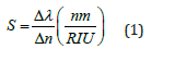
Figure 4:Reflection spectrum of the sensor for different values of DR.

In Table 1, the sensitivity of the sensor for different values of DR are summarized. These values are obtained for refractive index changes of Δn = 0.1.
Table 1:Sensitivity of the sensor for different values of DR.

Secondly, the diameter of the cavity located at the right part of the structure is changed from 660nm to 740nm with the steps of 20nm. The other geometrical parameters are DR=300nm and g=15nm. Figure 5 illustrates the reflection spectrum of the sensor for different values of DL. It is seen that the resonance wavelength is red-shifted for increasing the values of DL. The sensitivity of the sensor for these conditions is given in Table 2. The highest sensitivity is related to DL=740nm. It is due that the sensor has resonance at longer wavelengths by increasing DL. The higher the resonant wavelength, the higher the sensor’s sensitivity.
Figure 5:Reflection spectrum of the sensor for different values of DL.

Table 2:Sensitivity of the sensor for different values of DL.

The gap between the waveguides and cavities and also between the two cavities has a considerable effect on the behavior of the sensor. The gap determines the coupling efficiency between the waveguides and cavities. According to Figure 6, there is not a linear relationship between the increasing gap and the reflection spectrum of the sensor. However, the resonance dips in the reflection spectrum become narrower as the resonant wavelengths shift toward the shorter wavelengths. In Table 3, the sensitivity of the sensor for different values of g is expressed.
Table 3:Sensitivity of the sensor for different values of g.

Figure 6:Reflection spectrum of the sensor for different values of g.

As a refractive index sensor, the proposed structure must be sensitive to small changes in the refractive index in the etched regions. The dependency of the resonant wavelength on the refractive index changes is shown in Figure 7. The refractive index is increased from n=1 to n=1.1 with the steps of 0.02. The resonant wavelength and related reflection value for each value of n are given in Table 4. According to this Table, the sensitivity of the sensor with the geometrical parameters of DL=700nm, DR=300, g=15nm, and w=50nm is equal to 1560nm/RIU.
Table 4:Sensitivity of the sensor for different values of n.

Figure 7:Reflection spectrum of the sensor for different values of n.

Conclusion
In this work, a high-efficient MIM-based plasmonic refractive index sensor for use in the near-infrared region was presented. The effects of geometrical parameters on the reflection spectrum and the sensitivity of the sensor were studied using the 2D FDTD method. It was shown that the sensor’s sensitivity can be increased up to 1670nm/RIU by changing the geometrical variables of the structure. The total footprint of the sensor is 1.5μm2. The sensor can easily detect changes in the refractive index of about 0.02. High sensitivity, ultra-compact size, and detection of very small changes in the refractive index are advantages of the proposed sensor.
References
- Chen X, Liu Y, Huang J, Liu W, Huang J, et al. (2017) Label-free techniques for laboratory medicine applications. Frontiers in Laboratory Medicine 1(2): 82-85.
- Hunt HK, Armani AM (2010) Label-free biological and chemical sensors. Nanoscale 2(9): 1544-1559.
- Vestergaard MD, Kerman K, Tamiya E (2007) An overview of label-free electrochemical protein sensors. Sensors 7(12): 3442-3458.
- Maleki M, Mehran M, Mokhtari A (2020) Design of a near-infrared plasmonic gas sensor based on graphene nanogratings. JOSA B 37(11): 3478-3486.
- Verma R, Gupta BD, Jha R (2011) Sensitivity enhancement of a surface plasmon resonance-based biomolecules sensor using graphene and silicon layers. Sensors and Actuators B: Chemical 160(1): 623-631.
- Xie Y, Huang Y, Xu W, Zhao W, He C (2016) A plasmonic temperature-sensing structure based on dual laterally side-coupled hexagonal cavities. Sensors 16: 706.
- Tavousi A, Rakhshani M, Mansouri-Birjandi M (2018) High sensitivity label-free refractometer based biosensor applicable to glycated hemoglobin detection in human blood using all-circular photonic crystal ring resonators. Optics Communications 429: 166-174.
- Cotter D, Manning R, Blow K, Ellis A, Kelly A, et al. (1999) Nonlinear optics for high-speed digital information processing. Science 286: 1523-1528.
- Rezaei MH, Zarifkar A (2021) Realization of electro-optical decoder, half-adder, and half-subtractor using graphene plasmonic waveguides. Optical and Quantum Electronics 53: 297.
- Birr T, Zywietz U, Chhantyal P, Chichkov BN, Reinhardt C (2015) Ultrafast surface plasmon-polariton logic gates and half-adder. Optics Express 23: 31755-31765.
- Wu YD (2004) Nonlinear all-optical switching device by using the spatial soliton collision. Fiber and Integrated Optics 23: 387-404.
- Luo X, Qiu T, Lu W, Ni Z (2013) Plasmons in graphene: recent progress and applications. Materials Science and Engineering: R: Reports 74: 351-376.
- Rezaei MH, Zarifkar A, Miri M (2018) Ultra-compact electro-optical graphene-based plasmonic multi-logic gate with high extinction ratio. Optical Materials 84: 572-578.
- Alipour A, Farmani A, Mir A (2018) High sensitivity and tunable nanoscale sensor based on plasmon-induced transparency in plasmonic metasurface. IEEE Sensors Journal 18: 7047-7054.
- Khani S, Danaie M, Rezaei P (2019) Size reduction of MIM surface plasmon based optical bandpass filters by the introduction of arrays of silver nano-rods. Physica E: Low-Dimensional Systems and Nanostructures 113: 25-34.
- Zhu J, Lou J (2018) Ultrasensitive and multifunction plasmonic temperature sensor with ethanol-sealed asymmetric ellipse resonators. Molecules 23: 2700.
- Biswas S, Chakraborty J, Agarwal A, Kumbhakar P (2019) Gold nanostructures for the sensing of pH using a smartphone. RSC Advances 9: 34144-34151.
- Chen F, Zhang H, Sun L, Li J, Yu C (2019) Temperature tunable fano resonance based on ring resonator side coupled with a MIM waveguide. Optics & Laser Technology 116: 293-299.
- Rakhshani MR, Tavousi A, Mansouri-Birjandi MA (2018) Design of a plasmonic sensor based on a square array of nanorods and two slot cavities with a high figure of merit for glucose concentration monitoring. Applied Optics 57: 7798-7804.
- Shi X, Ma L, Zhang Z, Tang Y, Zhang Y, Han J, et al. (2018) Dual Fano resonance control and refractive index sensors based on a plasmonic waveguide-coupled resonator system. Optics Communications 427: 326-330.
- Chen Y, Chen L, Wen K, Hu Y, Lin W (2019) Double Fano resonances based on different mechanisms in a MIM plasmonic system. Photonics and Nanostructures-Fundamentals and Applications 36: 100714.
- Rakhshani MR, Mansouri-Birjandi MA (2018) A high-sensitivity sensor based on three-dimensional metal-insulator-metal racetrack resonator and application for hemoglobin detection. Photonics and Nanostructures-Fundamentals and Applications 32: 28-34.
- Rakhshani MR, Mansouri-Birjandi MA (2016) High-sensitivity plasmonic sensor based on metal-insulator-metal waveguide and hexagonal-ring cavity. IEEE Sensors Journal 16: 3041-3046.
- Rahman MZU, Krishna KM, Reddy KK, Babu MV, Mirza SS, et al. (2018) Ultra-wide-band band-pass filters using plasmonic MIM waveguide-based ring resonators. IEEE Photonics Technology Letters 30: 1715-1718.
- Guo Z, Wen K, Hu Q, Lai W, Lin J, et al. (2018) Plasmonic multichannel refractive index sensor based on subwavelength tangent-ring metal-insulator-metal waveguide. Sensors 18(5): 1348.
- Khani S, Danaie M, Rezaei P (2018) Realization of single mode plasmonic bandpass filters using improved nano disk resonators. Optics Communications 420: 147-156.
- Amoosoltani N, Mehrabi K, Zarifkar A, Farmani A, Yasrebi N (2021) Double-ring resonator plasmonic refractive index sensor utilizing dual-band unidirectional reflectionless propagation effect. Plasmonics 16: 1277-1285.
© 2023 Mir Hamid Rezaei. This is an open access article distributed under the terms of the Creative Commons Attribution License , which permits unrestricted use, distribution, and build upon your work non-commercially.
Editor In Chief


.jpg)


Signup for Newsletter

Quick Links
 Editorial Board Registrations
 Submit your Article
 Refer a Friend
 Advertise With Us
Our Recent Edition

.jpg)


Top Editors


.jpg)


.bmp)
.jpg)
.png)
.jpg)


.jpg)


.png)

.png)


.png)


Financial Support

Sponsors

Latest e-Books

Latest Video

 a Creative Commons Attribution 4.0 International License. Based on a work at www.crimsonpublishers.com.
Best viewed in
a Creative Commons Attribution 4.0 International License. Based on a work at www.crimsonpublishers.com.
Best viewed in