- Submissions

Full Text
Research & Development in Material Science
COP-free Effect Caused by Lowering Cross Point in a Dislocation-Free Ingot Grown by the NOC Method
Kazuo Nakajima1*, Masami Nakanishi2, Martin Su2 and Chuck Hsu2
1Emeritus Professor, IMR, Tohoku University, Japan
2GlobalWafers Co., Ltd. Hsinchu Science Park, Taiwan
*Corresponding author: Kazuo Nakajima, Emeritus Professor, IMR, Tohoku University, 2-1-1 Katahira, Aobaku, Sendai, 980-8577, Japan
Submission: May 22, 2023;Published: June 02, 2023
ISSN: 2576-8840 Volume 18 Issue 5
Abstract
A dislocation-free ingot was grown by the NOC method. The position of cross point between on centration curves of vacancy and interstitial Si atom was found to be a key factor for NOC growth to largely reduce COP caused by micro-void. Using this ingot, COP distribution was measured and COPs were confirmed not to exist in this wafer with the SC-1 cleaning in a Si ingot.
Keywords:COP; Void; Point defects; Dislocation-free; Diffusion; Single crystal growth; Growth from melt; Low-temperature region; Seed growth; Semiconducting silicon; Fine semiconductor technology
Introduction
The NOC (noncontact crucible) method has been proposed to grow Si single ingot with a large diameter ratio (diameter of ingot/diameter of crucible≒0.9) without contact with a crucible wall [1]. In this method, a large and deep low-temperature region was effectively established in a Si melt using an insulator plate set under the bottom of the crucible [2]. In the field of Si fine semiconductor, a COP (crystal originated particle)-free Si ingot is quite important because COPs become obstacles for the fine exposure technology of ultrafine semiconductor devices. We found that the position of cross point between concentration curves of vacancy and interstitial Si atom is a key factor and quite effective for NOC growth to largely reduce void formed by agglomeration of vacancies or COP caused by micro-void with the SC-1 cleaning in a Si ingot [3]. COP almost corresponds to void in this work. This may provide another method to obtain high-quality Si crystal in the field.
Growth of defect-free ingot by Cz (Czochralski) method
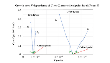
Figure 1 shows the concentration of vacancy, CV and interstitial Si atom, CI (z) near critical point as a function of growth rate, V. The temperature gradient, G is used as a parameter [4]. To reduce COP completely to 0, V/G or V or G must be controlled very precisely within quite narrow region closed to the critical point. Pv and Pi correspond to regions with quite low vacancy and interstitial Si atom, respectively. A defect-free crystal is made up of the Pv and Pi regions. This is the commonly used Cz method which requires precise controllability.
Figure 1:Cv and Ci concentration near critical point [4].
Growth and characterization of defect-free ingot grown by NOC method
Figure 2 shows a growing ingot inside low-temperature region in Si melt and the temperature gradient in the ingot [3,5]. As shown in Figure 2, the NOC method has the temperature gradient with two stages, G1 at the growing interface and G2 at the melt surface because the temperature gradient in the ingot should be largely changed at the melt-surface position from the gradual one to the steep one.
Figure 2:Schematic illustration of growing ingot and temperature gradients for the NOC method [3,5].
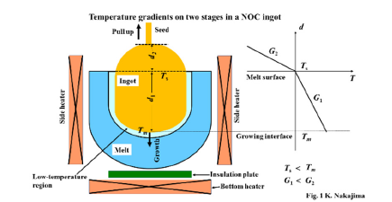
Figure 3 shows the schematic illustration of temperature gradients, CV and CI (z) in NOC and Cz ingots as a function of the distance from growing interface. The temperature gradient in the NOC ingot has a relatively gradual slope compared with that in the Cz ingot which grows above the melt surface [6].
Figure 3:Comparison between the temperature gradient, CV and CI in NOC and Cz ingots [3,5].
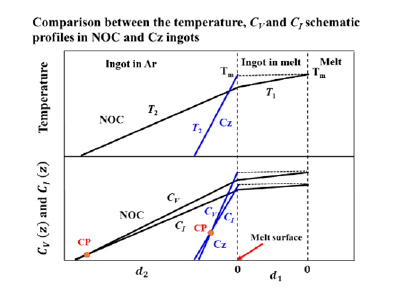
The position of cross point, CP between the CV (z) and CI (z) curves is quite important for NOC growth. The CP position for NOC growth is lower than that for Cz growth. To largely reduce COP in a Si ingot, the cross point should be largely lowered. Moreover, to almost completely reduce CV and CI in a Si ingot, the cross point should be lowered to the limit. The NOC method has a potential to largely lower the temperature of cross point. As the result, the residual defect concentration can be fundamentally approximated to zero. This is the simple mechanism to reduce COP to the limit in a NOC ingot.
A dislocation-free ingot was grown by the NOC method as shown in Figure 4; [4]. The length and diameter ratio are 15cm and 0.66, respectively. On the top part of ingot, four (111) facet planes were observed. Four liner habit lines appeared through the body to tail parts, which were clear evidence for dislocation-free. For more confirmation, no EPDs (etch-pit density of dislocations) were also observed at all over the ingot.
Figure 4:Dislocation-free NOC ingot [3].
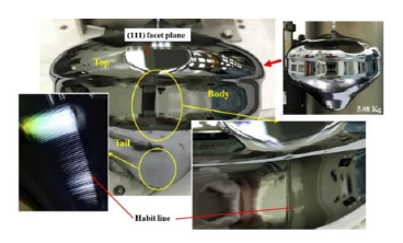
The CV at CP has possibility to be largely reduced by selecting proper ratio between the temperature gradients at the melt surface and at the growing interface using the NOC method [5]. For this ingot, from its cooling curve, vacancies in most parts of ingot can be regraded to be changed to voids near 1120 ℃ [7].
The distribution of BMD (Bulk Micro Defect: oxygen precipitate (SiO~<2) with stress in crystal), BSF (Bulk Stacking Fault: stacking fault caused by stress of excessive oxygen precipitate (SiO~2)) and OISF (Oxidation Induced Stacking Fault: stacking fault on (111) face caused by larger stress) in the cross section of the dislocationfree NOC ingot are shown in Figure 5. Many small white points and many a little bit long rod-shaped white points can be observed as BMD and BSF, respectively. The boundaries between BMD and BSF can be known by precise observation. A ring-OISF can be observed in the BSF region and is distributed along the periphery of ingot. The H band which contains BMD and BSF can be observed inside the ring-OISF, which is not shown in Figure 5.
Figure 5:Two-dimensional longitudinal distribution of BMD, BSF and OISF in the NOC ingot [3].
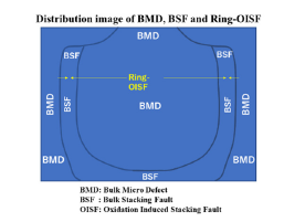
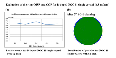
For the evaluation of COP, a B-doped (4.8mΩcm) NOC single wafer with 6φ inch was used. The distribution of COP was evaluated by the particle counter (counting size: 0.12μm) together with the SC (standard clean)-1 cleaning whose process was repeated 5 times. This cleaning process can little bit etch the surface of wafer. Figure 6(a) shows the trend of counting number. The particle counts more than 0.12μm and less than 0.16μm which corresponds to COP almost keeps constant after every cleaning. This means that COPs were not revealed from the inside wafer by the etching effect of the SC-1 cleaning because COPs did not exist inside this wafer.
Figure 6(b) shows the distribution of particles obtained by the particle counter for the same wafer after 5th etching. No particles larger than 0.12μm appeared all over the wafer. This also means COPs did not exist in this wafer. Quite few I-defects were also observed in the NOC ingot [3].
Figure 6:Distribution of COP in the NOC wafer [3].
Discussion
Advantages and disadvantages of the NOC method
The NOC mechanism to get COP-free ingot is more simple comparing to the Cz one. No precise control of V or G is required for NOC growth because lowering the cross point is only main factor to obtain such an ingot and it is more simple compared to keeping the critical point. Enough lowering the cross point can attain the complete and uniformly reduction of vacancy and interstitial Si atom. Only disadvantage of this method is the present furnace provides relatively lower growth rate.
Potential implication for the future semiconductor industry
When the future fine semiconductor industry will demand the more perfect Si crystal without distribution of the Pv and Pi regions which consist few vacancy and interstitial Si atom, respectively, the NOC method would be a strong candidate.
Conclusion
The mechanism to get COP-free ingot was proposed without precise control near critical point. It was proved by the growth of dislocation-free NOC ingot and the characterization about COP distribution over the ingot. The mechanism contains the position control of cross point which should be lowered to the limit. The ingot grown on this mechanism did not have COPs and had quite few I-defects. The present method has possibility to provide a way to obtain a Si ingot with uniformly and minimally distributed point defects. To largely increase the growth rate for practical use, how to maintain stability of the expanding rate will be important because the grow rate is limited by the expanding rate of low-temperature region in this method.
References
- Nakajima K, Ono S, Kaneko Y, Mura R, Shirasawa K, et al. (2017) Applications of novel effects derived from Si ingot growth inside Si melt without contact with crucible wall using noncontact crucible method to high-efficiency solar cells. J Crystal Growth 468: 705-709.
- Nakajima K, Ono S, Itoh H (2018) Concept and method to create a distinct low-temperature region in a Si melt for growth of a Si single ingot with a large diameter ratio using the noncontact crucible method. J Crystal Growth 499: 55-61.
- Nakajima K, Nakanishi M, Su M, Hsu C (2023) Two-dimensional BMD, BSF, ring-OISF and COP distributions in a dislocation-free ingot grown by the NOC method. J Crystal Growth 605: 127064.
- Nakajima K, Nakanishi M, Su M, Hsu C. COP-free effect of a dislocation-free ingot grown by the NOC method. Modern Chemistry & Applications.
- Nakajima K, Nakanishi M, Su M, Hsu C (2022) Two-dimensional distribution of vacancy concentration at cross points for the ingot length and the temperature gradients to largely reduce point defects and the growth of a dislocation-free NOC ingot for evaluation of its quality. J Crystal Growth 592: 126721.
- Nakajima K, Adachi T, Itoh H, Yang D (2019) Simulation to confirm the existence of distinct low-temperature regions in a Si melt using an insulating plate under the crucible bottom for the noncontact crucible method. J Crystal Growth 524: 125160.
- Nakamura K, Doctoral thesis for Tohoku University (2002) Study of diffusion of point defects in a single crystal of silicon during growth process and formation of secondary defects.
© 2023 Kazuo Nakajima. This is an open access article distributed under the terms of the Creative Commons Attribution License , which permits unrestricted use, distribution, and build upon your work non-commercially.
 a Creative Commons Attribution 4.0 International License. Based on a work at www.crimsonpublishers.com.
Best viewed in


.jpg)


 Editorial Board Registrations
 Submit your Article
 Refer a Friend
 Advertise With Us
.jpg)


.jpg)


.bmp)
.jpg)
.png)
.jpg)


.jpg)


.png)

.png)


.png)


