
- About Us
- Information
-

The Author ensures that the research has been conducted responsibly and ethically with adherence to all relevant regulations. read more..
- For Authors
- For Reviewer
- Manuscript Guidelines
- Membership
- Publication Ethics
-
- Journals
- Reprints
- e-Books
- Videos
- Policies
- Contact Us
 COVID-19
- Submissions


Full Text
Research & Development in Material Science
Electrical Conductivity and Dielectric Properties of Lead‑Free Perovskite: Ca0,08Na0,92Sn0,08Nb0,92O3 Ceramic
Abderrazek Oueslati*
Faculty of Sciences, University of Sfax, Tunisia
*Corresponding author: Abderrazek Oueslati, Laboratory for spectroscopic characterization and optics of materials, Faculty of Sciences, University of Sfax, Tunisia
Submission: December 01, 2020;Published: December 21, 2020

ISSN: 2576-8840 Volume 14 Issue 5
Abstract
The physical properties of the Multiferroïc Ca0,08Na0,92Sn0,08Nb0,92O3 ceramic were investigated by the X-ray Diffraction (XRD), morphology, piezoelectric, dielectric and electrical measurements. The X-ray diffraction patterns at room temperature revealed a single-phase perovskite crystallizing with quadratic P4mm group symmetry. The microstructural analysis shows the homogeneously grainy morphology of the compound with grain sizes varying from 2nm to 5.5nm. The piezoelectric responses were investigated as a function of temperature and frequency. The thermal evolution of the relative dielectric permittivity (ε'r) exhibited a very important peak with no frequency dependence, which revealed a classical ferroelectric behavior. So as to investigate the electrical transport, a complex impedance spectroscopy is highlighted. With the Debye theory-based analysis and a series of Arrhenius relations, the Nyquist plots are well suitable to an equivalent circuit model. Moreover, the conductivity spectrum exhibits the two phase transitions detected in the dielectric measurements.
Keywords: Ceramic compound; Piezoelectric study; Ferroelectric phase transition; Nyquist plots; Conductivity analysis
Introduction
Multiferroics are materials in which at the same phase there are at least two ferroic features, i.e., ferroelectricity and ferromagnetism or ferroelasticity [1,2]. The most interesting due to their potential applications are perovskite materials of the general formula ABO3. These materials are becoming increasingly widespread, such as in electronics, microelectronics, radiation detectors and electromechanical transducers [3-5]. In particular, there has been a growing interest in studying the Piezoelectric compounds mostly due to their properties such as the simplicity of crystallographic structure, their flexibility and their ability to change the physical characteristics by ionic substitutions on different structural sites. Especially, materials derived from sodium niobate NaNbO3 which are the subject of several studies due to their effective dielectric, piezoelectric, pyroelectric, and electro-optical properties [6]. These materials are widely studied as active materials in the acoustic domain, starting from the energy recovery to the actuator through the ink jet print head [7].
It is well-known that a suitable substitution on different atomic sites induces important modifications in the physico-chemical properties of the pure compound [8]. Therefore, it is of great interest to study the effect of the substitution in the A (Ca) and B (Sn) sites in NaNbO3 perovskite. We have synthesized and studied various properties of the ceramic compound, with the general formula Ca(1-x)Nax Sn(1-x)NbxO3 avec x=0.92. which is simplified by the expression CSNN0.92. This compound is crystallized in the quadratic system with P4mm space group, the unit cell parameters are a=b=3.9164Å, c = 3.9129Å and V=59.778Å3[9].
The aim of this research work is to synthesize the CSNN0.92 using a solid-state reaction by sintering at 1250K. Second, the crystal analysis of the sample by X-ray powder diffraction at room temperature is presented. The particle morphology of the powder is observed through EVO LS10 (Zeiss) scanning electron microscope. Finally, the piezoelectric measurements, dielectric and electrical properties of this ceramic compound are studied and discussed.
Experimental and computational method
Powder sample preparation: The polycrystalline sample of Ca0,08Na0,92Sn0,08Nb0,92O3 was prepared by the solid-state reaction method under high temperature. The ingredients taken to prepare the solid solution were highly pure (>99.9 %) AR grade precursor materials: CaCO3, Nb2O5, Na2CO3 and SnO2, all with required stochiometric. These precursors are carefully weighed into stochiometric proportions according to the following reaction
Afterwards, these forerunners were grinded for 1hour by an agate mortar. Then, methanol was added to have a homogeneous mixture that was then calcined in oxygen atmosphere at 1100 °C for 22h. After calcinations, powders have been mixed for 2hours, a few drops of polyvinyl alcohol (PVA) were added to the powdered sample for perfect binding. A second series of calcinations at 1100 °C for 48 hours was followed by 2 hours of sintering at 1250 °C (with a disk: 8mm in diameter and1 mm thick) (Figure 1)
Characterizations: In order to extract the crystalline structure, phase purity and lattice parameters in the obtained samples are characterized by an X-ray diffraction (XRD). The measurement is conducted at room temperature through CuKα radiation (=1.5406Å). XRD was analyzed by the Rietveld method using the “Fullprof’’ software [10] in the 2θ range of 10< 2θ<130 with a step scanning of 0.02.
The morphology of the obtained sample was analyzed by SEM, performed in a MEB PhilipsXL30 system, on the free surface of the material. The measurement was conducted in a high vacuum environment, using an electron beam accelerating with a voltage of 20kV.
Concerning the Piezo electric analysis, the measurements are extracted in a broad range of frequency and temperature using the impedance analyser (HP 4194A), to estimate both susceptance and conductance. The prepared sample was pressed through a hydraulic press into pellets of about 6.5mm diameter and 0.6mm thickness.
Figure 1: The pellets of the of CSNN0.92 compound.

Dielectric measurements were performed on sintered ceramic disks of 6.5mm diameter and 1mm thickness after the deposition of gold electrodes (600nm min-1 for 10min) on the circular faces by cathodic sputtering. The real and imaginary parts of relative permittivity εr’ and εr’’ were determined under a Helium atmosphere as a function of both temperature (300à 714K) and frequency (100Hz-200KHz) using a
Wayne-Kerr 6425 frequency analyzer.
The electrical measurements were performed using a two- electrode configuration on a polycrystalline sample. In fact, this compound was pressed into a pellet of 8mm diameter and 1.1mm thickness using 3t/cm2uniaxial pressure. On both sides of pellets, a thin layer of silver is deposited by thermal evaporation in order to insure an ohmic contact. These measurements were registered in a frequency ranging from 200 Hz to 5MHz with the SOLARTRON SI 1260 automatic bridge monitored by a microcomputer.
Results and Discussion
Crystalline parameters
The XRD pattern was analyzed to confirm the symmetry and to calculate the lattice parameters for CSNN0,92 compound. The values of the lattice and profile parameters were determined using a global profile matching method with the software “Fullprof”. Figure 2 shows a typical X-ray pattern at 300K, including the observed, the calculated profile and as well as the difference profile of the title compound. All the reflexion peaks of the X-ray profile were easily indexed in the quadratic structure belonging to the space group P4mm, and the refined unit cell parameters are a = b = 3.9164 Å, c = 3.9129Å and V = 59.778 Å3.These results are in agreement with the previously reported results for this compound [7]. The best refinements are listed in Table 1.
Table 1: The best refinements parameters of the CSNN0.92 ceramic compound.

Figure 2: X-ray diffraction pattern of a CSNN0.92 powder.

Figure 3a: SEM images for CSNN0.92 ceramic compound.

Figure 3b: Size distribution histogram with corresponding Gaussian fit for CSNN 0.92 ceramic compound.

Scanning Electron Microscope (SEM)
Figure 3a is the SEM image of the free surface of Ca0,08Na0,92Sn0,08Nb0,92O3 sample intered at 1250 °C for 2h. It consists of both large and small agglomerated grains characterized by a spherical shape only. The measurements and statistical evaluation of the grain size distribution were performed on many particles using the Image-J software. The results are displayed in Figure 3b as grain number (counts) versus particle size (nm). As it can be seen from this figure, the particles are reasonably monodisperse, and they are distributed according to a Lorentzian law (red solid line). The average diameter of the grain size is in the range of 2-5.5nm.
Piezoelectric measurements
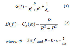
The Piezoelectric measurements were performed on disk shaped ceramics with CSNN0.92 at 155K, the conductance (G) and susceptance (B) were measured as a function of frequency around the main radial resonance mode (Figure 4). The material constants were computed using impedance equations and an equivalent circuit recommended by the IEEE Standard on Piezoelectricity [11]. It can be clearly seen that the magnitude of G and B increases with the increasing frequency. We can notice that the maximum of the conductance followed by a subsequent decrease of the susceptance at a particular frequency around 580KHz. This is the resonance frequency.
Figure 4: Variation of the admittance (G) and the susceptance (B) as functions of frequency At T =150K for CSNN0.92.

These curves have been fitted based on the following relationships:
The thermal evolution of the maximum susceptance (B(f)) in resonance is given in Figure 5. This figure shows that B(f) decreases gradually with the increasing temperature and disappeared near 265K. This observation indicates the presence of the phase transition, which is an agreement with the transition observed by the dielectric analysis in the simular compounds [6].
Figure 5: Temperature dependences for the conductance of the CSNN0.92 ceramic compound.

Figure 6: Variation of the susceptance (B) versus the admittance (G) of the CSNN0.92 ceramic compound.

Figure 6 shows the variation of the imaginary part of the admittance complex (B(f)) as a function of real parts (G(f)). It can also be seen in this figure that the variation is represented by a circle, which indicates the presence of a piezoelectric behavior of our developed compound [12]. In order to verify this behavior, we determine the piezoelectric parameters as a function of temperature, which are determined by the fitting of G and B.
The thermal evolution of the mechanical quality factor (Qm) is shows in Figure 7. This variation shows the presence of an extremum in the vicinity of 265K. This temperature verifies the approach of a phase transition, which is in good agreement with the transition obtained by the variation of the conductance as a function of the temperature. Moreover, it is well known that the factor has very high values which reflect the high loss dielectric in this material.
Figure 7: Thermal evolution of the mechanical quality factor of the CSNN0.92 ceramic compound.

The piezoelectric coefficients d31 and Kp as a function of temperature are plotted in Figure 8. It is seen that both coefficients drastically decrease as the paraelectric-ferroelectric transition temperature is approached. The decrease of d31 is due to the thermal agitations that are responsible for the disorder in this material.
Figure 8: Thermal evolution of the transverse piezoelectric coefficient and the planar coupling factor of the CSNN0.92 ceramic compound.

Dielectric studies
The temperature dependence of the real part of the relative dielectric permittivity (ɛ’r) in the frequency range from 1 to 100KHz is shown in Figure 9. Two dielectric anomalies have been observed, the first is detected at T=485K which indicates a phase transition and the second appeared at TC=635K which originated from a phase transition of a paraelectric to a ferroelectric phase. Moreover, the real part of the dielectric permittivity exhibits a sharp and narrow peak at Tc with no frequency dependence. This feature is typical of classical ferroelectrics [13,14]. Furthermore, the dielectric constant of a normal ferroelectric in the paraelectric region is generally known to follow the Curie–Weiss law described by the following equation [15]:
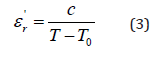
Where C is the Curie constant and T0 is the Curiee Weiss temperature.
Figure 9: Temperature dependence of the real parts of the relative dielectric constant.

Figure 10: Temperature dependence of ' 1 r ε at 1kHz and the fit to Curie Weiss law.

Figure 10 shows the variation of the inverse dielectric constant 1/ε'r as a function of temperature at 1kHz. The experimental data was fitted by Eq. (3) using a non-line are curve fitting method. The Fitted values parameters are the Curie constant C which was found to be 4.1365.104K, T0 =490K and TC =635245K. The no coincidence of TC and T0 implies that the phase transition is clearly of the first order [16]. The dependence of loss tangent (tanδ) of the title compound on temperature at some particular frequencies is represented in Figure 11. It is obvious that at low-temperature tanδ increases slowly, whereas in a high temperature region, it increases sharply. The scattering of a thermally activated charge carriers and/or defects generated during synthesis may be responsible for this sharp rise of tanδ for which the electrical conductivity also increases at high temperatures region.
Figure 11: Temperature dependence of tanδ at different frequencies of the CSNN0.92 ceramic compound.

Impedance analysis
The interface, grain and grain boundary properties are studied using the complex impedance formalisms that include the determination of capacitance, the relaxation frequency and the ionic conductivity [17]. The plot of -Z’’ versus Z’ (Nyquist diagram) at different temperatures of CSNN0.92 sample is shown in Figure 12. There are mainly two overlapping semicircles, which correspond to grain interiors (the semicircle at low frequency) and grain boundaries (the semicircle at high frequency) [18]. In other words, centers of semi circles that compose the total electric response are centered below the real axis (Z’), which confirms the presence of non-Debye type of relaxation in this compound. As can be seen in Figure 12, the diameter of the large semicircle arc of the impedance complex plane plot (Z*) decreased with the increasing temperature. This indicated that the total resistance decreased as temperature increased, which indicated, as a result, the existence of an activated conduction mechanism which confirms that the material behaves like a semiconductor.
Figure 12: Complex impedance plot of CSNN0.92 at various temperatures with equivalent circuit.

In order to analyze these spectra, it is useful to have an equivalent circuit model that provides a realistic representation of the electrical properties of the respective regions. Therefore, these data were successfully fitted, by using Zview software, to an equivalent circuit consisting of a series of combinations of grain and grain boundary elements. The First consists of a parallel combination of resistance (Rg), capacitance (Cg) and a constant phase element CPEg. The second consists of a parallel combination of resistance (Rjg) and a constant phase element CPEjg (Figure 11).
The impedance of the CPE contribution is an empirical function of the type:
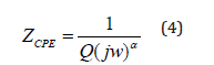
Where ω is the angular frequency, Q indicates the value of the pseudo-capacitance of the fractal interface CPE element, and αrepresents the magnitude of the departure of the electrical response from an ideal condition and also indicates the degree of depression of arc below the real axis. In order to check the choice of the equivalent circuit, we present in Figure 13 the variations of the experimental values of Z′ and Z′′ at some temperatures versus the simulated ones calculated using the parameters extracted from the equivalent circuit. It is obvious from this figure that the slope obtained from a fit linear of the data points at each temperature is nearly equal to the unity. This behavior indicates that the adopted equivalent circuit describes the electric properties of the investigated compound.
Figure 13: Plots of measured values versus simulated values of the real and imaginary parts of the impedance.

Relying on the bulk resistance values and the sample dimensions, the grain electrical conductivity can be calculated at each temperature using the following equation:
Where: e and S are respectively the thickness and the area of the pellet.
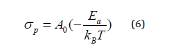
The temperature dependence of the conductivity (Ln (σpT)) versus 1000/T) is shown in Figure 14. Besides, the experimental values of conductivity are fitted to the Arrhenius-type comportment described by the following expression:

Figure 14: Plot of Ln (σT) versus (1000/T) of the conductivity data for CSNN0.92 ceramic compound.

Where A is the pre-exponential factor, k is the Boltzmann constant and Ea is the activation energy.
All phase transitions appearing in dielectric study are affirmed by the change of the curve slope at T1 and T2. The values of the activation energy determined from a linear fit to the data points are Ea(I) = 0,48eV in region I, Ea(II) = 0,59eV in region II and Ea(III) = 0.77eV in region III.
Conclusion
In summary, A lead free piezoelectric perovskite solid solution CSNN0.92 is synthesized using the solid-state reaction method. An X-ray structural analysis confirms that this material displays the quadratic structure in a P4mm space group at room temperature. The micro structural analysis shows the homogeneously grainy morphology of the compound with grain sizes varying from 2nm to 5.5nm. The piezoelectric measurements were carried out to complement the understanding of the materials’ behavior. The evolution of the real part of dielectric permittivity and dielectric loss (tanδ) versus temperatures revealed a anomaly at 635K that corresponds to the ferroelectric-paraelectric transition temperature. The investigations on the impedance further reveal that (i) the electrical conduction in the material contributed by both the grain and the grain boundary effect, (ii) the material behaves like a semiconductor.
References
- Aliouane K, Guehria-Laidoudi A, Simon A (2005) Study of new relaxor materials in BaTiO3-BaZrO3-La2/3TiO3 J Solid State Sci 7(11): 1324-1332.
- Aydi A, Khemakhem H, Boudaya C, Simon A (2005) X-ray and dielectric studies of ferroelectric or relaxor phases in the Ca1 – xNaxSn1 − xNbxO3 J Solid State Sci 7(3): 249-255.
- Razak KA, Asadov A, Yoo J, Haemmerle E, Gao W (2008) Structural and dielectric properties of barium strontium titanate produced by high temperature hydrothermal method. J Alloys Compd 449(1-2): 19-23.
- Khemakhem L, Maalej, Kabadou A, Ben Salah A, Simon A, et al. (2008) Dielectric ferroelectric and piezoelectric properties of BaTi975(Zn1/3Nb2/3)0.025O3ceramic. J Alloys Compd 452(2): 441-445.
- Moura F, Simões AZ, Stojanovic BD, Zaghete MA, Longo E, et al. (2008) Dielectric and ferroelectric characteristics of barium zirconate titanate ceramics prepared from mixed oxide method. J Alloys Compd 462: 129-134.
- Benabdallah F, Aydi A, Abdelmoula N, Khemakhem H, Simon A, et al. (2012) Dielectric, pyroelectric and piezoelectric properties in the (1-x)(0.1BaTiO3-0.9NaNbO3)-xLiNbO3 J Solid State Sci 14: 1333.
- Hamdi O, Mighri F, Rodrigue D (2018) Piezoelectric cellular polymer films: Fabrication, properties and applications. J Aims Materials Sci 5(5): 845-869.
- Amouri A, Aydi S, Abdelmoula N, Dammak H, Khemakhem H (2018) Evidence of magnetoelectric coupling in 0.9BiFeO3-0.1Ba[Ti95(Yb0.5Nb0.5)0.05]O3ceramic. J Alloys Compd 739: 1065-1079.
- Aydi A, Chkoundali S, Khemakhem H, Simon A, Muhll R (2008) X-ray diffraction, dielectric measurements and Raman spectroscopy: : Studies of the (1-x)CaSnO3-x NaNbO3 solid solution. J Alloys compd 465(1-2): 222-226.
- Rodriguez-Carvajal J (1998) Program Full Prof, Laboratoire Léon Brillouin (CEA-CNRS) Version 3.5d - LLB - JRC.
- Singh V, Kumar H, Kharat D, Hait S, Kulkarni M (2006) Effect of lanthanum substitution on ferroelectric properties of niobium doped PZT ceramics. J Materials Letters 60(24): 2964-2968.
- Aydi A, Simon A, Michau D, Von Der Muhll R, Abdelmoula N, et al. (2011) Elaboration and dielectric study of ferroelectric or relaxor ceramics in the ternary system BaTiO3-NaNbO3-BaSnO3. J Alloys Compd 509(29): 7773-7777.
- Zouari I, Abdelkafi Z, Seveyrat L, Sassi Z, Perrin V, et al. (2017) Improved piezoelectric and electro-caloric effects in the BaTi 975(Nb0.5Yb0. 5) 0.025 O3 lead-free ceramic characterized by phase-coexistence at room temperature. J Mate Chem Phy 200: 121-127.
- Aydi S, Nouiri M, Aydi A, Khemakhem H (2015) Structural and dielectric studies of ferroelectric or relaxor ceramicsin the Ca1-xNax(Ti5Sn0.5)1-x NbxO3 system. Ceram Int 41(10): 13607-13613.
- Ma J, Liu X, Zhou C, Yuan C, Minhong L (2014) Enhancement of the dielectric, piezoelectric, and ferroelectric properties in BiYbO3-modified (Ba85Ca0.15)(Ti0.9Zr0.1)O3 lead-free ceramics. Ceram Int 40(2): 2979-2984.
- Taub J, Ramajo L, Castro MS (2013) Phase structure and piezoelectric properties of Ca-and Ba-doped K1/2Na1/2NbO3 lead-free ceramics. Ceram Int 39(4): 3555-3561.
- Cross LE (1987) Relaxor ferroelectrics. Ferroelectrics 76: 241
- Enneffati M, Louati B, Guidara K, Rasheed M, Barillé R (2018) Crystal structure characterization and AC electrical conduction behavior of sodium cadmium orthophosphate. J Mater Sci: Mater Electron 29: 171-179.
© 2020 Abderrazek Oueslati. This is an open access article distributed under the terms of the Creative Commons Attribution License , which permits unrestricted use, distribution, and build upon your work non-commercially.
Editor In Chief


.jpg)


Signup for Newsletter

Quick Links
 Editorial Board Registrations
 Submit your Article
 Refer a Friend
 Advertise With Us
Our Recent Edition

.jpg)


Top Editors


.jpg)


.bmp)
.jpg)
.png)
.jpg)


.jpg)


.png)

.png)


.png)


Financial Support

Sponsors

Latest e-Books

Latest Video

 a Creative Commons Attribution 4.0 International License. Based on a work at www.crimsonpublishers.com.
Best viewed in
a Creative Commons Attribution 4.0 International License. Based on a work at www.crimsonpublishers.com.
Best viewed in