- Submissions

Full Text
Research & Development in Material Science
Preparation of GaSe Nanorods Sensor by Liquid Phase Exfoliation
Ganlin Chen and Wanqiang Cao*
School of Materials Science and Engineering, Hubei University, China
*Corresponding author: Wanqiang Cao, Hubei Key Laboratory of Polymer Materials, School of Materials Science and Engineering, Hubei University, Wuhan 430062, China
Submission: October 02, 2019;Published: October 15, 2019

ISSN: 2576-8840 Volume12 Issue1
Abstract
GaSe nanorods were synthesized by liquid phase exfoliation as a resistive switch memory device with a transverse graphene/GaSe/graphene structure. The mechanism is the charge trapping/detrapping effect.
Keywords: Liquid phase exfoliation; Nanorods; Resistive switching
Introduction
The semiconductor GaSe belongs to a two-dimensional layered structure, and the p-type semiconductor with a band gap varying from 2.1eV to 3.5eV [1]. As high optical responsivity and high external quantum efficiency [2], it can be used for photodetectors [3]. The traditional liquid phase exfoliation will reduce the purity of material device, because organic solvent has a higher boiling point. Controlling the growth of high-quality two-dimensional selenide crystals has become a key problem [4]. In present work, GaSe nanorods were synthesized by liquid phase exfoliation as a resistive switch memory device with a transverse graphene/ GaSe/graphene structure.
Experimental
The GaSe bulk was added to a mixed solution of isopropyl alcohol and deionized water, and subjected to insert shear stirring, followed by ice bath ultrasonication, and centrifuged at 10,000rpm. The GaSe suspension was deposited on a SiO2/Si substrate containing graphene. The morphology of GaSe was tested by scanning electron microscope (SEM, XL30 SFEG, FEI), and Transmission electron microscopy (TEM, Tecnai G2 20 U-TWIN TEM). Raman analysis was carried out on micro-Raman spectrometer using an excitation wavelength of 532nm. The current-voltage characteristics.
Results and Discussion
Figure 1:SEM images of GaSe nanostructures obtained at centrifugation speeds of 10000rpm.
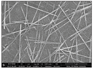
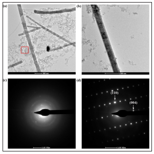
In Figure 1, the nanoflakes are stacked on a plane with some nanorods of 8-14μm in length. Figure 2(a) & 2(b) show the typical bright-field TEM images for the nanostructures and a specific nanorod with a higher magnification. Selected area electron diffraction (SAED) patterns are shown in Figure 2(c) & 2(d). The polycrystalline rings indicate many GaSe nanoflakes with different orientations gathering together. The SAED pattern of the single nanorod in Figure 2(d) shows only one set of diffraction spots of six-fold symmetry, which conforms to the space group P-6 of hexagonal GaSe, indicating that single crystalline GaSe nanorods with hexagonal symmetry have been successfully synthesized.
Figure 2:(a) and (b) Bright-field TEM images of GaSe nanostructures. (c) and (d) SAED pattern for the square area in (a) and the single nanorod in (b), respectively.
The device structure is shown in Figure 3(a), and Raman shows in Figure 3(b) the four modes were detected for bulk GaSe at 134.8cm-1 (A11g), 209.5cm-1 (E21g), 244.0cm-1 ( E12g), and 304.6cm-1 (A12g), consistent with the vibration modes previously reported. Two A1g peaks are the out-of-plane vibrational mode of GaSe, while E2g and very weak E1g peaks correspond to the in-plane mode [5-8].
Figure 3:(a) Device setup with structure of graphene/GaSe/grapheme; (b) Raman spectra of bulk GaSe and GaSe nanostructures; (c) I−V characteristic of graphene/GaSe; (d) Double-log I-V curve of the device.
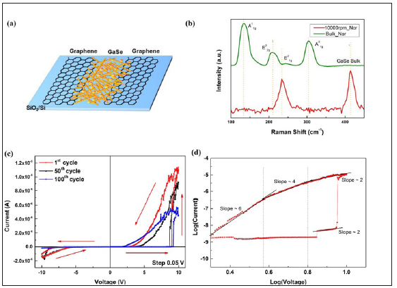
The nonlinear rectification behavior of the device is demonstrated in Figure 3(c) that a dipole layer is formed at the graphene/GaSe interface with charging effect [9]. An ON/OFF ratio above 104is achieved from the I-V curve of the device, and the device operates well throughout over 100 cycles of ON/OFF without severe degradation. The double logarithmic I-V curve of Figure 3(d) is explained as the charge trapping/detrapping effect. When the wells in the channel are filled, the injected charges are trapped as the voltage increases, accompany a sudden increase in current and switching from OFF to ON state.
Conclusion
The GaSe nanorods having the memory effect were prepared by the liquid phase exfoliation.
References
- Bergeron A, Ibrahim J, Leonelli R (2017) Oxidation dynamics of ultrathin GaSe probed through Raman spectroscopy. Applied Physics Letters 110: 1625-1654.
- Zhou Y, Nie Y, Liu Y (2014) Epitaxy and photoresponse of two-dimensional GaSe crystals on flexible transparent mica sheets. ACS Nano 8(2): 1485-1490.
- Li X, Lin M W, Puretzky AA (2014) Controlled vapor phase growth of single crystalline, two-dimensional GaSe crystals with high photoresponse. Scientific Reports 4.
- Mcmanus D, Vranic S, Withers F (2017) Water-based and biocompatible 2D crystal inks for all-inkjet-printed heterostructures. Nature Nanotechnology 12(4): 343-350.
- Huang H, Wang P, Gao Y (2015) Highly sensitive phototransistor based on GaSe nanosheets. Applied Physics Letters 107(14): 143112.
- Lu R, Liu J, Luo H (2016) Graphene/GaSe-nanosheet hybrid: Towards high gain and fast photoresponse. Scientific Reports 6(1): 19161.
- Hu PA, Wen Z, Wang L (2012) Synthesis of few-layer GaSe nanosheets for high performance photodetectors. ACS Nano 6(7): 5988-5994.
- Mahjouri-Samani M, Tian M, Wang K (2014) Digital transfer growth of patterned 2D metal chalcogenides by confined nanoparticle evaporation. ACS Nano 8(11): 11567-11575.
- Si C, Lin Z, Zhou J (2016) Controllable schottky barrier in GaSe/graphene heterostructure: the role of interface dipole. 2D Materials 4(1): 015027.
© 2019 Wanqiang Cao. This is an open access article distributed under the terms of the Creative Commons Attribution License , which permits unrestricted use, distribution, and build upon your work non-commercially.
 a Creative Commons Attribution 4.0 International License. Based on a work at www.crimsonpublishers.com.
Best viewed in


.jpg)


 Editorial Board Registrations
 Submit your Article
 Refer a Friend
 Advertise With Us
.jpg)


.jpg)


.bmp)
.jpg)
.png)
.jpg)


.jpg)


.png)

.png)


.png)


