
- About Us
- Information
-

The Author ensures that the research has been conducted responsibly and ethically with adherence to all relevant regulations. read more..
- For Authors
- For Reviewer
- Manuscript Guidelines
- Membership
- Publication Ethics
-
- Journals
- Reprints
- e-Books
- Videos
- Policies
- Contact Us
 COVID-19
- Submissions


Full Text
Research & Development in Material Science
Design, Realization and Characterization of a Wide-Angle Microwave Metasurface Absorber
Emiliano Sassolini1, Maria Denise Astorino1, Muhammad Khalid1, Enrico Lia1, Marco Muzi1, Patrizio Simeoni2, Nicola Tedeschi1, Andrea Veroli1, Alessandro Simonetto3 and Fabrizio Frezza1*
1Department of Information Engineering, Electronics and Telecommunications, Italy
2National Transport Authority (NTA), Ireland
3IFP-CNR Milano, Italy
*Corresponding author: Fabrizio Frezza, Department of Information Engineering, Electronics and Telecommunications, Sapienza University of Rome, Rome, Italy
Submission: August 30, 2019;Published: September 12, 2019

ISSN: 2576-8840 Volume11 Issue4
Abstract
In this article, we present a metamaterial absorber (MMA), and more specifically a metasurface based on a periodic structure consisting of double split-ring resonators (dSRR) which efficiently absorbs electromagnetic radiation for a wide range of incidence angles for both the transverse electric (TE) and the transverse magnetic (TM) polarizations. The proposed unit cell was designed employing a full 3-D electromagnetic solver based on the Finite Element Method (FEM). The unit cell consists of a square splitring resonator and a thin metallic plate separated by a dielectric layer. Investigations of parameterization and optimization have shown that small modifications in the geometry of the resonator led to enhanced angular absorption. The numerical simulation stage was followed by design and fabrication of a prototype containing several unit cells. The measurements on the prototype show an absorbance peak larger than 84% and 58% for the incidence angles θ=0˚ and θ=70˚ respectively, at 9.73 GHz. The proposed MMA and its variations enable numerous applications such as defense systems, communication and stealth technologies.
Keywords: Periodic structure; Split-ring resonator; Unit cell; Wide-angle absorbance; Metasurface
Introduction
The term metamaterial generally refers to a kind of structures artificially designed to obtain physical and chemical properties difficult to find in nature [1,2]. Assembled in a fashion of composite materials such as metal and dielectric parts, they are usually arranged in periodic structures. Their shape, geometry, size, orientation and arrangement give them properties capable of manipulating electromagnetic waves, by blocking, absorbing or bending waves in ways not achievable with conventional materials [3,4]. In the electromagnetic applications, metamaterials usually consist of periodic sub-wavelength metallic elements. For example, electric ring resonators arrays (ERR) on a dielectric substrate can exhibit very different performances for light modulation, such as abnormal refraction and electromagnetic wave absorption. Landy et al. [5] have theoretically and experimentally presented the metamaterial absorbers (MMAs) in 2008 [5], which have proven to be the best candidate for a wide range of applications, the most popular include sensor application [6,7], low radar cross section devices [8,9] and electromagnetic stealth technology [10,11], feature of extreme interest for the modern military defense. The study of MMAs is recently the topic of interest of a large number of research institutes, especially in order to find new concept designs for the unit cell and new solutions for fabrication technology. For the X-band frequencies, Sood and Tripathi show an inclined hexagonal patch [12], Nguyen and Lim introduce an eight-resistive-arm for broadband and different angle absorption [13]. 3D-printing technique has introduced new fabrication perspectives, such as low-cost printed MMA [14] and hexagonal three-dimensional honeycombs [15]. Furthermore, different kinds of materials are used: an electro composite MMA was produced in composite material consisting of spherical carbonyl iron and multiwall carbon nanotubes [16] and even distilled water as substrate array to thermally tune the MMA from S-band to Ku-band [17]. Lastly, MMAs have been proposed also in the THz-regime, where complete new approaches have been explored: for instance Deng et al. [18] introduced a tunable MMA based on liquid crystal [18], Fu et al. [19] theoretically studied a MMA based on multi-layer graphene [19] and Astorino et al. [20] proposed a potentially flexible polyimide based ultra-thin narrow-band MMA [20]. The goal of this research is to highlight in detail the entire design process of a wide incidence angle-insensitive MMA consisting of a double split-ring resonator and a thin metallic plate separated by a dielectric layer. Aimed at a working frequency in X-band region and in particular from 9.5 to 10GHz, the device was designed and manufactured in Arlon material. Arlon fiberglass laminate for microwave application is typically used for the fabrication of antennas [21], and recently proved to represent a good choice as a metamaterial substrate [22]. Finally, its compatibility with the standard micro-fabrication techniques is well suited for an inexpensive metamaterial prototype.
After this first, introductory section, the paper presents six further sections: in the second section, the design and simulation results of the MMA are reported, the third section illustrates the parameterization study and optimization process, employing a numerical simulation tool. The prototype fabrication and measurement set-up are then described in section four. The fifth section covers the results and finally the sixth section is reserved to the discussion and future development.
Materials and Methods
In this study, we propose an MMA designed, optimized and manufactured according to the six-step process illustrated in Figure 1.
Figure 1:Process followed in the design of the presented MMA.

The structure is conceived to manipulate the electric and magnetic resonances independently, therefore both incident electric and magnetic fields are absorbed. The proposed MMA resonator unit cell is presented in Figure 2a. It is made of a square split-ring resonator and a thin metallic plate as a ground plane, separated by a dielectric layer, inspired by the design presented by Landy et al. [5], but having some differences in the geometry, in the ground-plane (a metal strip is present in [5]) and in the material employed that allowed to achieve a large angular absorbance, in particular for the TE mode. The MMA has been designed for manufacturing in a commercial Polytetrafluoroethylene (PTFE) based laminate, AR450 by Arlon Inc., for applications with a relative dielectric constant (εr ) of 4.50 and loss tangent of 0.0035 at 10 GHz. The copper foil thickness chosen for the resonator and metallic plate is 1 oz. (35 micron). The nominal dielectric constant tolerance of 0.30 is tighter than for typical thermoset grades, assuring more consistent performance. Another significant advantage offered by these products includes the loss tangent performance a designer would expect with PTFE-based laminates, up to an order of magnitude better than thermoset resin-based materials. In terms of numerical simulation, a full 3-D electromagnetic solver (CST Studio Suite) based on the Finite Element Method (FEM) is used to design, parameterize and optimize the unit cell. A second electromagnetic tool (COMSOL Multiphysics) is also used in order to benchmark and confirm the results given by CST Studio Suite.
The optimum resonator unit cell is composed by two identical split ring resonators made by a copper foil (35µm thick) with arms forming a meander line in a square shape (W=4.50mm, T=0.25mm, H=3T), see Figure 2. A gap (G=0.30mm) is located along the main axis (y) of the resonator geometry, providing a capacitive coupling that actuates in one of the transverse resonant modes. The bottom side is fully covered by a metal copper foil plate (L=11.50mm, 35µm thick) acting as a ground plane, therefore reducing the transmittance parameter. Due to the symmetry with respect to the x- and y- directions, the device is expected to provide absorption for both transverse electric (TE) and transverse magnetic (TM) waves. In the simulation environment, the x and y boundaries of the unit cell are chosen to be periodic whereas the z boundaries are left open. The incident plane wave is defined using Floquet ports. The solver enables an arbitrary number of Floquet modes to be defined for each port. In the simulation environment only two modes are chosen as the incident plane wave is defined by the very first Floquet mode. The cell boundary condition virtually repeats the modelled structure periodically in the xy plane to infinity. Figure 2b shows the tetrahedral mesh refinement for the unit cell with a total of 137.528 tetrahedrons, and in Figure 2c the cell boundaries for the unit cell are depicted, where the upper and lower z boundaries are left open to receive the incident TM and TE waves.
Figure 2:(a) Unit cell and its dimensions. (b) Tetrahedral mesh refinement for the unit cell. The mesh cell dimensions adapted in the frequency sweep. (c) Cell boundaries for the unit cell.

For an MMA, there are three key aspects to be investigated: absorbance, reflectance and transmittance, which are intrinsically related to one another. Absorbance (A) is defined as the ratio of absorbed radiant power to incident radiant power. The transmittance (T) is defined as the ratio of transmitted radiant power to incident radiant power and reflectance (R) is the ratio of reflected radiant power to incident radiant power. Being defined as ratios of radiant power values, absorbance, reflectance and transmittance are dimensionless and can also be expressed in terms of percentage, therefore the relationship holds: T + R + A = 1 or 100%. These parameters, as a function of the angular frequency ω, are related to the scattering parameters and are given by the following relationship:
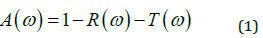
where R(ω)=|S11|2 and T (ω)=|S21|2 are obtained through either simulation or measurement. The aim of a good MMA is to obtain very small values of reflectance and transmittance at the design frequency. A negligible magnitude of T(ω) can be obtained using a full metal plate with thickness greater than the skin depth at the bottom side of the MMA structure. Figure 3a shows the simulated results of the split-ring resonator for A(ω), R (ω) and T(ω) in the condition of normal incidence for the TE and TM waves, with the dimensions displayed in Figure 2a and using the proposed Arlon substrate AR450.
From Figure 3a, and due to the symmetry in the x- and y-directions of the MMA structure displayed in Figure 2, two resonances for the TE and TM waves appear. For the TE wave, it is R= 0.392% and T= 0.001%, giving A= 99.607%, while for the TM wave, it is R=6.304% and T=0.001%, giving A=93.695%. Respectively, in terms of S-parameters in dB scale, two resonance peaks are displayed in Figure 3b. For the TM wave, a peak of -12.00dB appears at 8.412GHz and for the TE wave, a peak of -24.10dB appears at 9.502GHz.
Figure 3: (a) Simulated response of the Absorbance, Reflectance and Transmittance of the MMA for the TE and TM waves. (b) S11 scattering parameter in dB scale with resonance peaks at 8.412GHz and 9.502GHz for TM and TE waves, respectively.

Figure 4 shows the angular responses as a function of incidence angle θ with the azimuthal angle φ at 0˚ and 90˚, for both TE and TM polarizations. The simulated results demonstrate a wide-angle behavior of the absorbance levels: in the case of φ=0˚ (Figure 4a), the absorbance at θ=70˚ reaches a value of 50% and 90% for TE and TM modes, respectively, while in the case of φ=90˚ (Figure 4b), the absorbance reaches a value of 70% and 100% for TE and TM modes. The equivalent electrical circuit representing the unit cell and its relevant response for both resonances in the TE and TM waves are illustrated in Figure 5 & 6.
Figure 4:Angular responses of Absorbance, Reflectance and Transmittance of the MMA for the TE and TM waves as a function of the incidence angle θ with (a) φ=0˚ and (b) φ=90˚, where φ is the azimuthal angle.

Figure 5:The equivalent electrical circuit of the unit cell.

Figure 6:The response of the equivalent electrical circuit of the unit cell.

Parameterization and optimization
In order to investigate a possible enhancement in the performance of the MMA, aiming at effective absorption (A) at wide angles, a parameterization study and an optimization process were carried out. The purpose of the parameterization study is to find one or more parameters with enough degree of freedom that are effective in obtaining the desired results. It also intends to minimize the number of parameters to be set in the optimization process, lest a huge computational effort is needed with a risk of not obtaining convergence. The degree of freedom established for each parameter is also used to scale the geometric properties of the unit cell. The parameterization is set individually to each parameter in the simulation environment, assigning a variable to each one and using the parameter sweep function. Another benefit of the parameterization is to find the correct response in the simulation environment with respect to the measurements which are function of the tolerance of the material employed in the design of the MMA.
The following variables were defined for the parametric study:
1. Substrate relative dielectric constant (sweeping εr from 4.2 to 4.8, as the tolerance of AR450 is ±0.30)
2. Resonator gap distance (sweeping G from 0.28 to 0.32mm)
3. Resonator square size (sweeping W from 4.20 to 4.70mm)
4. Resonator line width (sweeping T from 0.22 to 0.27mm)
After the parameterization study, we could determine a number of variables that are effective in achieving the target performance set. First, the substrate dielectric constant shifts the resonant frequency. Increasing εr lowers frequency and vice-versa. Second, the resonator gap distance G, acting as a capacitance and providing coupling within the arms of the unit cell, influences the resonant frequency (a larger gap width lowers frequency), therefore a tradeoff is established between the desired frequency and the amount of absorption of the incident wave. While increasing G, the resonance frequency is lowered but coupling is also affected, worsening the absorption ratio. The opposite provides over-coupling, also worsening the absorption ratio. The third conclusion relates to the resonator square size (W) that mainly determines the resonant frequency without influencing much the absorbance. As W increases, the resonance frequency is increased and vice-versa, while absorption barely improves. Lastly, the resonator line width (T) influences the resonant frequency and absorption ratio. As T increases, the absorption rate also increases. However, this parameter has to be kept under control to work within the X-band region, since the resonance frequency is lowered.
The main targets set within the optimization process are then defined as:
1. Good absorption on both TM and TE waves (symmetry of unit cell)
2. Wide incident-angle absorption (>90% over 70◦)
3. Wide-band operation frequency (> 50MHz)
In conclusion, a trade-off between the absorption ratio and angular response is obtained with the variables W and T: the optimum combination for those parameters was found W=4.50mm and T=0.25mm. The critical coupling is obtained with the resonator gap parameter G equal to 0.30mm. The relative dielectric constant, εr, initially set to 4.50 as an input from the nominal value of the AR450 material, was later adjusted to 4.25 to match the measured results, still within its tolerance of 0.30. In conclusion, this combination of parameter values was found adequate for prototyp fabrication.
Fabrication and measurement set-up
To manufacture the MMA, we synthesized 53x39 unit MMA cells by using standard printed-circuit board fabrication techniques. The fabrication process flow is the following: first the optical resist AM140 EIDA is deposited on the copper film, then a Laser Direct Imaging (LDI) is performed using an Orbotech Paragon 9800I instrument with the CAD-CAM masking design, at the end a copper wet-etching process is carried out in ammonia solution. The manufactured MMA is shown in Figure 7a & b. Measurements at normal incidence were made in a monostatic arrangement, using a 125x100mm pyramidal horn antenna, initially placed at 300mm from the sample under test, connected to an AB Millimetre MVNA8- 350 Vector Network Analyzer (VNA) through an adapter and a 10 dB directional coupler. A scheme of the measurement setup is shown in Figure 7c. Free-space calibration was made with the same technique as in [23,24]: a motorized linear stage controlled by the VNA moved the target along the line of sight by a half wavelength while taking data at constant frequency. Given the small extent of the movement, target illumination by the antenna does not change significantly, and one can safely assume that only the phase of the wave reflected from the target is changed. The (complex) amplitude of the reflected wave (S11 scattering parameter) traces a circular path in the complex plane while the target is moved. The radius of the circle is proportional to the target reflectivity, whereas the center is related to systematic errors. The measurement is repeated on the target and on a flat mirror of the same size, assumed fully reflecting. In this case, the metamaterial sheet was reversed, using its ground plane backing as a mirror. The (scalar) target reflectivity is computed by the ratio of the radii of the two circles. This calibration technique can no longer be used in a bistatic arrangement, as necessary for oblique incidence, since moving the target along a line would also cause transverse displacement in this case. A simple response correction was thus applied, using the ground plane backing as the fully reflecting reference and using a semi-anechoic environment to reduce stray reflections. This procedure has limited accuracy and may account for discrepancies with calculations at non-normal incidence.
Figure 7:The final manufactured MMA. (a) Total panel surface; (b) Optical image of a single unit cell. (c) Scheme of a measurement set-up environment.

Results
The measurements performed, in TE polarization, are illustrated here. The band of interest is 8-12GHz where the simulations show a strong resonance absorption. Figure 8 shows the normal-incidence measurement result of S11 for the TE wave polarization, compared with simulations: the reflectivity resonance peak at 9.73GHz is -8.23dB, corresponding to 85% of total absorbed radiation in contrast to the value of 99.72% of absorption found in simulations; the simulation shows a resonance peak at 9.50GHz with εr = 4.5 while the measurement yields resonance at 9.73 GHz: such a value of the resonance can be obtained in the numerical setup by imposing εr =4.25; this value of the relative permittivity is within the tolerance of the chosen material, so it is natural to suspect that this shift is simply due to a deviation of the relative permittivity, allowed by the material tolerances.
Figure 8:Comparison between simulation and experimental measurement (S11) spectra under normal incidence in TE polarization.

Only one measurement session could be allocated, and an approximately symmetrical range was chosen around the TE design frequency. For the oblique incidence the reflectivity has been acquired at the incidence angles θ= 20, 30, 40, 50, 60, and 70 degrees. The trend of the absorbance for the different angles is reported in the Table 1. The behavior of these parameters shows that a minimum of the absorption occurs around 9.73GHz, but also evidences discrepancies with simulations.
Table 1:Comparison between simulated and measured absorbance at different incident angles

For the normal-incidence configuration, the frequency discrepancy between simulation and measurements, as seen, can potentially be explained with the relative dielectric constant. We used for the relative dielectric constant a value of 4.5 in simulations, but the datasheet of Arlon AD450 gives a tolerance of ±0.30, so the dielectric constant can vary between 4.2 and 4.8. Another simulation sweep for values in that range showed that for εr =4.25 the frequency peak is 9.73GHz. The other discrepancy in the absorption values cannot be only addressed to a different permittivity value and could be ascribed to manufacturing issues that show some differences between the ideal simulated device and the measured prototype.
Discussion
In the present work, we have analyzed, fabricated and measured a microwave metamaterial absorber synthesized in Ar lon AD450 material. AD450 is a material with a dielectric substrate thickness of 0.51mm, εr = 4.50, between two copper layers. One layer holds the electric ring resonator and the other acts as a metallic mirror. The choice of material offers the advantage that the entire device can be manufactured using the classical printed-circuit board fabrication methods and therefore it can be easily integrated into more complex systems making the proposed MMA an inexpensive and reliable technology. The device has been designed by FEM methods in order to reach the maximum absorption peak at 9.73GHz for normal incidence and wide-angle absorption. The prototype was characterized in a monostatic configuration for normal incidence and a bi-static configuration for incidence at different angles. The measurement results confirm, at normal incidence, an absorption resonance around 9.70GHz, with a small shift within the tolerance of the substrate dielectric constant. As seen, we found other differences in absorption between simulation and measurement, that we think could be caused by the natural discrepancies between the simulated device and the fabricated one, even though more analyses will be required to fully understand the aforementioned discrepancies. The characterization at oblique incidence shows a good absorption level but, again, there is a divergence from the numerical results that may be due either to fabrication or measurement setup: to address this, further investigation will be required. In terms of future developments and research, other degrees of freedom can be further exploited, since absorption at wide angles increases proportionally with substrate thickness; also, the choice of a thicker copper foil can increase resistive losses which will also improve the overall absorption. Another degree of freedom lies in the geometry of the resonator unit cell, that can be further improved. Since the resonator geometry is planar, interaction with electromagnetic waves at wide angles is poor, therefore the inclusion of via holes in the design as 3-D shape in combination with a thicker substrate may significantly improve the absorbance at wide angles.
References
- Veselago VG (1968) The electrodynamics of substances with simultaneously negative values of ε and µ. Soviet Physics Uspekhi 10(4): 509-514.
- Smith DR, Pendry JB, Wiltshire MCK (2004) Metamaterials and negative refractive Science 305(5685): 788-792.
- Astorino MD, Frezza F, Tedeschi N (2017) Ultra-thin narrow-band, complementary narrow-band, and dual-band metamaterial absorbers for applications in the THz regime. J Appl Phys 121(6): 063103.
- Grady NK, Heyes JE, Chowdhury DR, Zeng Y, Reiten MT, et al. (2013) Terahertz metamaterials for linear polarization conversion and anomalous refraction. Science 340(6138): 1304-1307.
- Landy NI, Sajuyigbe S, Mock JJ, Smith DR, Padilla WJ (2008) Perfect metamaterial ab Phys Rev Lett 100(20).
- Bakir M, Karaaslan M, Akgol O, Altintas O, Unal E, et al. (2018) Sensory applications of resonator-based metamaterial Optik 168: 741-746.
- Cong L, Tan S, Yahiaoui R, Yan F, Zhang W, et al. (2015) Experimental demonstration of ultrasensitive sensing with terahertz metamaterial absorbers: A comparison with the metasurfaces. Appl Phys Lett 106(3): 031107.
- Li M, Xiao SQ, Bai YY, Wang BZ (2012) An ultrathin and broadband radar absorber using resistive IEEE Antennas Wirel Propag Lett 11: 748-751.
- Liu T, Cao X, Gao J, Zheng Q, Li Q, Yang (2013) RCS reduction of waveguide slot antenna with metamaterial IEEE Trans Antennas and Propag 61(3): 1479-1484.
- Schurig D, Mock JJ, Justice BJ, Cummer SA, Pendry JB, et al. (2006) Metamaterial electromagnetic cloak at microwave frequen Science 314(5801): 977-980.
- Pan G, Zhu J, Ma S, Sun G, Yang X (2013) Enhancing the electromagnetic performance of Co through the phase-controlled synthesis of hexagonal and cubic Co nanocrystals grown on graphene. ACS Appl Mater Interfaces 5(23): 12716-12724.
- Sood D, Tripathi CC (2016) A wideband wide-angle ultrathin low profile metamaterial microwave Microwave and Optical Technology Letters 58(5): 1131-1135.
- Nguyen TT, Lim S (2018) Design of metamaterial absorber using eight-resistive-arm cell for simultaneous broadband and wide-incidence-angle absorption. Scientific Reports 8(1): 6633.
- Yoon Y, Lim D, Tentzeris MM, Lim S (2018) Low- cost metamaterial absorber using three-dimensional circular truncated Microwave and Optical Technology Letters 60(7): 1622-1630.
- Jiang W, Yan L, Ma H, Fan Y, Wang J, et al. (2018) Electromagnetic wave absorption and compressive behavior of a three-dimensional metamaterial absorber based on 3D printed Scientific Reports 8(1): 4817.
- Huang Y, Song WL, Wang C, Xu Y, Wei W, et al. (2018) Multi-scale design of electromagnetic composite metamaterials for broadband microwave absorption. Composites Science and Technology 162: 206-214.
- Shen Y, Zhang J, Pang Y, Zheng L, Wang J, et al. (2018) Thermally tunable ultra-wideband metamaterial absorbers based on three-dimensional water-substrate construction. Scientific Reports 8(1): 4423.
- Deng G, Lu Y, Yin Z, Lai W, Lu H, et al. (2018) A tunable polarization- dependent terahertz metamaterial absorber based on liquid crystal. Electronics 7(3): 27.
- Fu P, Liu F, Ren GJ, Su F, Li D, et al. (2018) A broadband metamaterial absorber based on multi-layer graphene in the terahertz Optics Communications 417: 62-66.
- Astorino MD, Fastampa R, Frezza F, Maiolo L, Marrani M, et al. (2018) Polarization-maintaining reflection-mode THz time-domain spectroscopy of a polyimide based ultra-thin narrow-band metamaterial Scientific Reports 8(1): 1985.
- Leonardi O, Pavone M, Cadili T, Sorbello G, Isernia T (2013) Monolithic patch antenna for dedicated short- range communications. Electronics Letters 49(2): 85-86.
- Vivek A, Shambavi K, Zachariah CA (2016) Simulation study of ENG based metamaterial Proceeding of the 2016 International Conference on Control, Instrumentation, Communication and Computational Technologies (ICCICCT), Kumaracoil, India, IEEE, pp. 353-357.
- Murk A, Duric A, Patt F (2008) Characterization of ALMA calibration targets. Proceeding of the 19th International Symposium on Space Terahertz Technology, Groningen, The Netherlands, pp. 530-533.
- Murk A, Duric A (2007) ALMA calibration device proto- type calibration load test IAP Research Report, Bern, Switzerland.
© 2019 Fabrizio Frezza. This is an open access article distributed under the terms of the Creative Commons Attribution License , which permits unrestricted use, distribution, and build upon your work non-commercially.
Editor In Chief


.jpg)


Signup for Newsletter

Quick Links
 Editorial Board Registrations
 Submit your Article
 Refer a Friend
 Advertise With Us
Our Recent Edition

.jpg)


Top Editors


.jpg)


.bmp)
.jpg)
.png)
.jpg)


.jpg)


.png)

.png)


.png)


Financial Support

Sponsors

Latest e-Books

Latest Video

 a Creative Commons Attribution 4.0 International License. Based on a work at www.crimsonpublishers.com.
Best viewed in
a Creative Commons Attribution 4.0 International License. Based on a work at www.crimsonpublishers.com.
Best viewed in