- Submissions

Full Text
Research & Development in Material Science
A Superior Mechanical Property Nanocrystalline Diamond Film for Extremely Thin Terahertz Traveling Wave Tube Window
Ming Q Ding*, Lili Li, Chengyi Hua, Xinghui Li, Lin Chen, Pan Pan, Xianping Wu, Jun Cai and Jinjun Feng
Beijing Vacuum Electronics Research Institute, China
*Corresponding author:Ming Q Ding, National Key Laboratory of Science and Technology on Vacuum Electronics, Beijing Vacuum Electronics Research Institute, Beijing, China
Submission: August 05, 2019;Published: August 09, 2019
ISSN: 2576-8840 Volume11 Issue3
Abstract
A high quality freestanding nanocrystalline diamond (NCD) film grown in a microwave plasma CVD system has been studied and applied in extremely thin terahertz traveling wave tube windows. An average fracture strength from the 100~260μm thick freestanding films was found to be ~1814MPa, showing superior mechanical strength. A seven-layered 60μm microcrystalline diamond (MCD)/NCD composite film was fabricated for 850GHz traveling wave tube (TWT) windows. Then window components were assembled using laser cut MCD/NCD disks without lapping or polishing. The tests of the window showed this extremely thin MCD/NCD film meets the requirements for mechanical and vacuum properties of the window, while CST simulated bandwidths were found to be about 44.2GHz and 71.4GHz for the return loss ≤-30dB and -20dB, respectively. The results of this study demonstrate the NCDs grown at the relatively low CH4/H2, and high substrate temperature possess superior mechanical properties at least comparable to ultra-nanocrystalline diamonds (UNCDs) and thus can be employed in fabrication of the extremely thin composite diamond for THz TWT windows. This novel process of MCD/NCD and MCD/ UNCD composite diamond films provides a practical method for the fabrication of extremely thin THz TWT windows.
Keywords: Nanocrystalline diamond (NCD); Mechanical property; Air-tightness; Extremely thindiamond window; Terahertz traveling wave tubes
Introduction
In the past decades, Nanocrystalline diamond (NCD) and Ultrananocrystalline diamond (UNCD) films have been exploited intensively due to their wide variety of applications in several areas, such as heat spreading, tribology, biology, micro/nano-technology [1-10], and composite diamond windows for traveling wave tubes (TWTs) [11,12]. While UNCDs are reported to have smaller average grain sizes from ~20nm down to ~5nm, reported grain sizes of NCDs vary enormously from ~20nm to hundreds of nm, featuring a variety of properties. A popular approach for the growth of NCD films is to employ a relatively high CH4/H2 ratio (≥5%) and low substrate temperature (Ts <800 ℃), in a CVD system. Under such conditions, re-nucleation is believed to dominate the growth process that diamond grain size can be maintained at around 20nm or even smaller [13].
Though the low Ts process enables utilizing various types of substrates, such a process is likely at the expense of the film’s properties, such as poor mechanical properties resulting from high defects and increased sp2 carbon content in the grain boundaries. For example, Reinhard et al. reported a low Yang’s modulus of 710GPa for the NCD film grown at 2.7kPa, compared to a high value of 1015GPa of one grown at 4.4kPa and 100 ℃ higher [14]. The Raman spectra from NCD and UNCD are often found to be dominated by the G-band (sp2 bonding), especially under low Ts (below~700 ℃) and microwave power [13-15]. Zeng et al. [10] studied sp2 content in boron-doped NCD synthesized with an H-rich gas system using Near Edge X-ray Absorption Edge Fine Structure (NEXAFS) technique. They found an increase of the sp2 content from 3.2±0.6% to7.6±0.9% when the substrate temperature decreases from 750-800 ℃ to 460 ℃, but a much large value of 54%±2% at temperature of 850 ℃.
Although there have been a large number of studies on Properties of thin NCD films, a few studies are concerned with mechanical properties of freestanding thick NCDs. In particular, there is lack of data regarding mechanical properties of the freestanding NCD films grown under relatively low CH4/H2 ratio, and high temperature.
One of the objectives of this study is to develop a microwave plasma CVD (MPCVD) process for the fabrication of freestanding NCD films featuring superior mechanical properties and low microwave loss, compared to or even better than UNCDs. To do so, a number of freestanding NCD films with thickness up to 260μm, grown at possibly low CH4/H2 of 2-3.5% and high Ts of 855-890 ℃ in a MPCVD system, have been investigated. The more important objective of the study is to apply the optimized NCD process to the fabrication of MCD/NCD composite diamond films for the extremely thin THz traveling wave tube (TWT) windows.
THz wave sources have several potential applications, such as THz spectroscopy [16,17], imaging [18,19], wireless communication [20], security inspection [21] and Radars [22,23]. Among a few types of THz sources including solid state and photonic devices, THz traveling wave tubes are considered to be promising in terms of their capability to offer relatively high radiation power. With the frequencies approaching THz region, characteristic dimensions of the TWT components become much smaller, making the fabrication rather challenging. As one of the key components of the TWT, the window assembly needs to be not only air-tight but also capable to transmit THz waves efficiently. To reduce the wave, return lossmajor loss of the diamond window, the required thickness of the THz wave window could be down to tens of μm [12]. This brings about an issue of mechanical strength of the window against atmospheric pressure difference. For such thin windows, even MCD does not have adequate mechanical strength and air tightness due to MCD large grain size. Therefore, single-crystalline diamond (SCD) has been used to fabricate the THz TWT windows [24,25]. However, the cost of the SCD windows would be high due to the low fabrication efficiency of thin SCD disks. On the other hand, we have proposed a novel MCD/UNCD composite diamond film for high frequency TWT windows [11,12]. Though UNCD has been used successfully in the multilayered MCD/UNCD film, the growth conditions of UNCD differ substantially from those of MCD. On the contrary, NCD and MCD have very similar growth parameters, thus the use of high quality NCDs, instead of UNCDs, would greatly facilitate the fabrication process of the composite films. In addition, as an excellent structural material, such high-quality freestanding NCD films would also have potential applications in some other components or devices.
Experimental Procedures
Fabrication of the NCD film
Diamond films of NCD, MCD and UNCD were fabricated using a 6kW, 2.45GHz microwave plasma reactor [26]. Both NCD and MCD were grown in H-rich H2/CH4 gas mixture, while UNCD was grown in a Ar-rich gas mixture. All the films were prepared on N-type (100) silicon wafers with a diameter of 40mm. Prior to diamond deposition, the silicon substrate was mechanically polished with 0.3 μm diamond powder, attaining a nucleation density of ~1x10¹¹/cm3 for NCD and UNCD growth. Relatively thick NCD films up to 260μm were prepared under CH4/H2 ratio 2-3.5%, microwave power (Pp) 1.7-2.0kW, pressure (P) 17.3-18.6 kPa and Ts of 855-890 ℃. The Silicon substrate was finally etched away leaving freestanding diamond films for the experimental study and property tests. The morphology of the NCD films was examined using a highresolution scanning electron microscopy (HRSEM) (Hitachi-4800). Raman spectroscopy and X-ray diffraction (XRD) were employed to characterize the structure of the NCD film while XRD was also employed to estimate the film’s internal stress.
Morphology of the NCD film
Since for TWT window materials, vacuum-tightness is one of the basic requirements, cross-section morphology of the NCD film has been examined. Figure 1 gives a cross-section SEM image of the 70μm thick NCD grown at 3% CH4/H2. It is seen that the entire cleaved section, from the bottom to the top, consists of densely packed nano-granules (≤20nm).
Figure 1:A cross-section SEM image of the 70μm thick NCD, showing densely packed ≤20nm nanogranules from the bottom to the top.
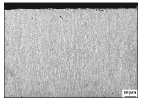
Figure 2:A cross-section SEM image from interface area between UNCD and MCD, showing similar grain size (≤ ~20μm) and structure.
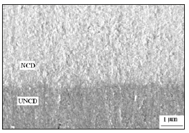
For morphology comparison with UNCDs, a 50μm thick NCD was grown on a 3μm UNCD that was prepared at CH4/H2/ Ar=1.2/6/243sccm, Ts 820 ℃, Pp =1.5kW and P=12kPa. Figure 2 shows a cross-section SEM image from the interface region, where a bright NCD layer sits on the top of a dark UNCD. There is hardly any difference between the two regions in terms of grain size and diamond crystalline structure. The image from these two layers, however, reveals sharp contrast. This is believed to be due to distinct hydrogen content in NCD and UNCD as well as on their cleaved surface, as reported in [27,28], which results in difference in surface electron negative affinity.
Structure of the NCD film
Raman spectra were taken using 532nm laser (Horiba T6400) to identify the structure of the NCD films. Figure 3 displays three Raman spectra respectively from: (a) a UNCD grown at CH4/H2/ Ar=1.2/6/245sccm, (b) a NCD grown at 3% CH4/H2, (c) a NCD grown at 2% CH4/H2. As seen from the figure, the spectra (b) and (C) exhibit five main peaks at 1120, 1332, 1350, 1450 and 1547cm- 1, featuring typical characteristics of NCDs. All the features look very similar to those of the UNCD spectrum (Figure 3a) in terms of peak position and shape appearance, except that diamond peak (1332cm-1) of the NCDs is clearly resolved compared to that of the UNCD. In fact, all studied NCD films reveal well-defined diamond peak of 1332cm-1, particularly the film grown at 2% CH4/H2, which may result from the relatively low CH4/H2 and other processing parameters, such as relatively high Ts and P used in this work. It is known that the presence of the diamond feature is indicative of high quality of the NCD with low sp2 content [13], which is beneficial to the THz wave windows in terms of low wave transmission loss. D-band of the feature 1547cm-1 seems shifted towards low wave number, compared to 1580cm-1 usually reported.
Figure 3:Raman spectra from: (a) the UNCD grown at CH4/H2/Ar=1.2/6/245sccm, (b) the NCD grown at 3% CH4/H2, and (c) the NCD grown at 2% CH4/H2.
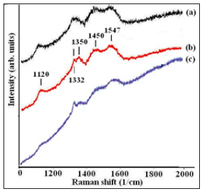
Figure 4:A typical XRD patterns taken from the NCD films grown at 2%CH4/H2.

The NCD structure was also studied by XRD. Figure 4 shows a typical XRD patterns taken from the NCD film grown at 2% CH4/H2. As seen from the patterns, there are only three major visible peaks representing the (111), (220) and (311) lattice planes of diamond, and no other irrelevant peaks are observed, which confirms the high quality of the NCDs, with no larger graphite precipitates. Among three peaks, the (220) one has the highest intensity, indicating a (110) preferred orientation. Its 2θ values representing inter-plane distances will be employed to calculate the internal stress below.
Results and Discussion
Mechanical properties of the NCD film
Stress estimated from XRD: Given that large internal stress of the NCD film would ruin its mechanical properties, particularly for a freestanding structural material that is likely to become bowed or even cracked, the internal stress of the NCD films was studied using XRD data.
The inter-plane distance of a diamond film, d, can be calculated from the Bragg diffraction formula:
2d sinθ=λ
Where θ is the angle between the incident X-ray and the diamond surface, and λ is the wavelength of the incident X-ray. According to the Hooke’s law, the internal stress σ is proportional to the strain of the film, and given by
σ=E(d-d0)/d0
where E is the Young’s modulus, and d0 is the inter-plane distances of a given lattice plane in the natural diamond. As the reported Young’s moduli of the NCD films vary from about 510 to over 1000GPa [14], a higher E value of 1000GPa was taken for calculation of the internal stress σ.
Figure 5:The calculated internal stress σ as a function of the growth rate and CH4/H2 ratio of the NCD films, grown at Ts 855 ℃, P 17.4kPa and Pw 1.7kW with CH4/H2 ratio varying from 2% to 4%.
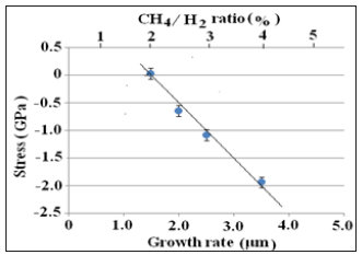
Figure 5 displays the calculated internal stress σ as a function of the growth rate and CH4/H2 ratio for four NCD films, which all were grown at Ts 855 ℃, P=17.3kPa and Pp =1.7kW with CH4/H2 ratio varying from 2% to 4%. It can be seen that, when the growth rate is greater than 1.5μm/h, the films exhibit compression stresses that increase linearly with a rise in growth rates and CH4/H2 ratio, while at around 1.5μm/h the film approaches a near-zero tensile stress of 39±92MPa. These stress findings are in agreement with the observed curvature of the freestanding samples.
The compression stress in diamonds has been widely reported for UNCDs and NCDs [29,30]. This is because, in most cases, excessive CH4 is used as to achieve high growth rates and small grain sizes. However, high CH4/H2 ratio are likely to incorporate more sp2 carbon into the film resulting in compression stresses. The results of the stress values vs. growth rates, together with Raman data, indicate the growth rate of ~1.5μm/h (2% CH4/H2) is preferred in order to produce a high quality NCD film with near-zero stress and low sp2 carbon content.
Fracture strength vs thickness: To measure NCD fracture strength Fs, several NCD films at growth rate of 1.5-3μm/h were fabricated and at least four test samples were laser cut for each NCD film. A three-point bending tester that is able to accommodate relatively small area samples-typically ~5x2mm2, was employed to measure Fs based on the following formula [31]:
Fs=3PL/2wD2
where, P is fracture force measured from a three point bending test, L, distance between two support point, w and D, width and thickness of the tested diamond slab, respectively.
Figure 6:Measured Fs values as a function of NCD thickness (blue diamond), the red square representing a 140μm composite, with 40μm NCD on 100μm MCD.
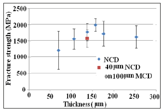
Figure 6 shows the measured fracture strength Fs as a function of thickness D of the NCD films (blue diamond) and the fracture strength for a total thickness 140μm composite of NCD/MCD (red square). An overview of the Fs vs D plot is that measured data are quite scattered with relatively large average errors, resulting from lack of ductility or yielding of the material from which the fracture strength is mainly determined by defect size [32]. For individual Fs measurements, a highest Fs value of 2890MPa was found. It is also noted from Figure 6 that the Fs values do not show obvious dependence on thickness, such as a drop with the increasing film thickness as reported by Coe et al. [33]. This may be due to fact that our test samples are NCD rather than MCD. Unlike MCD, the NCD grain size remains unchanged through the growth process as discussed in Section 2.2, therefore larger flaws or defects are not likely to occur even in the thick NCD film, resulting in independency of the fracture strength on NCD thickness. However, for the 70μm film, the measured Fs data are relatively small and exhibit much larger average errors-up to ±586MPa. Interestingly, for the 60μm thickness MCD/UNCD composite film in our previous studies, such measurements failed since the sample was too thin for the fracture force P to be measured [12]. Therefore, a film’s thickness of 70μm seems close to the low measurement limit for the three-point bending test, leading to rather poor measurement accuracy.
To further explore the effect of diamond film thickness on fracture strength measurements, a composite film with 40μm NCD over-layered on 100μm MCD was fabricated. The measured Fs of 1560±228MPa (red square in Figure 6) is obtained by simply assuming D=140μm (a total thickness). It is interesting to note that the Fs value is reasonably close to that of the pure NCD with the same thickness, and even closer to the value of 1550±150MPa for a 100μm composite film of MCD/UNCD as reported in our previous study [12]. This finding manifest that the surface layer of tested diamond films plays a major role in against the fracture force. On the other hand, the finding also verifies the rather poor measurement accuracy for the 70μm pure NCD film due to inadequate thickness. By excluding the Fs data of the 70μm NCD film, an average Fs value of the NCDs is found to be ~1812 MPa, showing a superior mechanical strength.
By comparison, the above overall Fs data are comparable to those of UNCDs (2.52, 1.34 and 1.50GPa for three samples), and higher than those of three NCDs (0.82, 1.3 and 1.6 GPa), measured by Reinhard et al. using ~1 μm thick membranes [14]. They are also higher than our previous data obtained from MCD/UNCD composite films [12]. Of course, our Fs data are far lower than those (2.92-5.03GPa), measured by Espinnosa et al. [32] from thin UNCD membranes [32]. which are the highest ever reported. It should be noted our samples for the measurements are much thicker than theirs, which may be one of the reasons for the large difference in Fs values. Furthermore, the measured Fs data of the NCDs do not exhibit obvious effect of growth rates or stress of the NCDs, for which further work is needed.
Application of the NCD in composite diamond windows for THz TWTs
Design and fabrication of the multilayered MCD/NCD composite diamond: Based on the previous work of the MCD/ UNCD composite windows [12], we properly redesigned a MCD/ NCD structure, as to maximize NCD’s mechanical advantages while minimizing its disadvantages-forward wave loss from small amount of sp2 carbon atoms.
To improve the strength of the nucleation side for the MCD/ NCD, the thickness of the NCD layers in the composite is minimized to 0.5μm, while the thickness of the bottom NCD layer is increased to 4.5μm, and further measures will be described in the fabrication process below. Reducing the thickness of the internal NCDs is because their main role is to improve surface roughness of the composite by holding the growing MCD grains. In fact, regarding surface roughness, a proper one, e.g. Ra=~200-500nm, was found to be beneficial to having strong adhesion between diamond and metallization layers for the vacuum-tight window brazing, compared to that in the case of low surface roughness, e. g. ≤tens of nm.
Figure 7:A schematic drawing of a designed MCD/NCD composite film with total thickness of 60μm, consisting of seven layers (from bottom to top): NCD1(4μm), MCD1(17μm), NCD2(0.5μm), MCD2(16.5μm) and NCD3(0.5μm), MCD4(16.5μm) and NCD1(4.5μm).

Figure 7 gives a schematic drawing of a seven-layered MCD/NCD composite film with total thickness of 60μm that was optimized for 850GHz TWT windows. It can be seen that three thick MCD and two thin NCD layers are sandwiched between two relatively thick NCD layers. The total thickness of the NCD layers is ~10μm, which would bring about an acceptable level of forward wave loss [12,34].
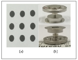
Figure 8:(a) laser cut Ø2.68 disks, an (b) photos of a assembled window component for the testing, taken from two directions.
The fabrication of the MCD/NCD film began with mechanically polishing a Ø40mm silicon (100) substrate to attain a high nucleation density (up to ~1x10¹¹/cm2). The diamond growth process follows the designed drawing shown in Figure 8, starting from the bottom NCD layer, then the first MCD and so on. The process sequence and detailed growth parameters for MCDs and NCDs are listed in Table 1. The growth conditions of the NCD were selected based on the above studies for the high quality NCD film with superior mechanical strength, and low internal stress and sp2 carbon content.
Table 1:The process sequence and detailed growth parameters for MCDs and NCDs

The transition between NCDs and MCDs can be readily programed and quickly implemented due to the same gas mixture used, compared to that for the MCD/UNCD composite. The thickness of each layer is achieved by controlling the growth period of time that was calculated from the growth rate.
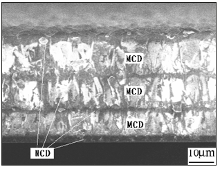
A freestanding Ø40mmx60μm MCD/NCD film was fabricated, with its Cross section SEM image shown in Figure 9. Though not each layer’s thickness is exactly the same as designed, the overall structure is reasonably well. Since the mechanical strength values from the nucleation side of NCDs or UNCDs were found to be less2 than 1GPa, about 50% lower than those from the growth side, the film’s nucleation surface was H-plasma etched to remove the defect-rich layer (about 2μm) and then regrown with a 2μm NCD film. Experimental tests on thicker films showed that the Fs values of the regrown nucleation surface increased by an average value of ~450 MPa, indicating a substantial improvement.
Figure 9:Cross section SEM image of a fabricated 60μm thick MCD/NCD film with four layers of NCDs and three layers of MCDs.
The composite diamond film was laser cut into Ø2.68mm window disks without lapping or polishing, as shown in Figure 8(a). The rim of the disks on both sides were then undergone the processes of metallization before brazed onto two frames to form a pillbox type of the window assembly. Figure 8(b) shows a photo of the window component with the window in the middle of the component. It should be noted that the structural design of the window assembly including the selection of the window thickness was conducted using CST simulation, with some of the simulated results described in Section 3.3.3.
Mechanical and vacuum tests: Since the MCD/NCD film was too thin to be measured due to the limit of the minimum detectable fracture force. Therefore, the MCD/NCD window conponent (Figure 8(b)) was employed to test the window’s mechanical strength and vacuum tightness against atmospheric pressure. After connecting the component to the testing chamber of a leak detector, a vacuum was quickly attained. The detected maximum air leakage of the whole window was found to be ≤1x10⁻⁹Pa.l/s with no any cracking or other damages, indicating its adequate mechanical strength and air tightness of the window disk. The testing result confirms the MCD/NCD film satisfies the requirement of vacuum-tightness and the minimum thickness Dmin for a window disk, which is correlated to mechanical strength Fs measured as fracture strength, given by [35]
Dmin=0.55D’(ΔP.SF/Fs)1/2
Where, D’ is the diameter of the window disk, Δp is the pressure difference between two sides, and SF is the safety factor set to 4.
Figure 10:A physical model of the window assembly for CST simulation.

Simulation of the return loss vs frequency: Apart from the mechanical and vacuum properties, RF property, in particular the return loss, is another most important one for the THz window. Currently it is impossible to test RF properties of the window assembly at 850GHz due to unavailability of the testing system. Instead, the return loss vs. frequency is simulated using the CTS code. Figure 10 gives a physical model of the window assembly, which consists of upper rectangle and circular wave guides, a window disk and lower rectangle and circular wave guides. The simulated results with 60μm thick disks showed that the broad frequency bandwidths could be achieved for the low return loss. Figure 10 shows two curves of return loss vs. frequency, where the bandwidths were found to be about 44.2GHz and 71.4GHz for the return loss ≤-30 dB and -20 dB, respectively. Though this excellent RF property is unable to be verified by testing, the simulated results are believed rather accurate and reliable judging from previous studies on lower frequency TWT windows [11]. Nevertheless, RF properties of the window need to be verified by testing the assembled TWT in the near future (Figure 11).
Figure 11:Return loss vs Frequency of the window assembly, showing broad bandwidths at lower return loss: (a) 44.2GHz for return loss≤-30dB and (b)~71.4GHz for return loss ≤-20dB.

Conclusion
We have prepared high quality freestanding nanocrystalline diamond films in a MPCVD system. The cross-section SEM image shows the 70μm thick NCD film consists of densely packed nanograins from the bottom to the top surface. From Raman spectra, all the NCD films exhibit a well-defined diamond peak of 1332cm-1, indicating high quality of the NCDs with relatively low sp2 carbon content. The measured average fracture strength from the 100- 260μm thick freestanding films was found to be ~1814MPa, featuring a superior mechanical strength, compared to those of the UNCD reported in our previous work. It is believed the above properties of the NCD is associated with the relatively low CH4/H2 and high Ts used in this study, and beneficial to the fabrication of extremely thin diamond windows.
To demonstrate the high quality of the NCDs, a multi-layered MCD/NCD composite film with total thickness of 60μm was designed and fabricated for 850GHz TWT windows. The growth conditions for the NCD layers were optimized for low stress and sp2 carbon content, and high strength. Finally, a window component using the MCD/NCD film was fabricated and tested. Mechanical and vacuum tests show this MCD/NCD film has the adequate mechanical properties for the extremely thin THz TWT windows. In terms of the requirement of the minimum thickness Dmin as well as air tightness for a window disk material, we believe the MCD/NCD window disk thickness may be further reduced from 60μm down to about 40μm or less. Currently, though single crystalline diamond is an alternative for the extremely thin windows, the lapping and polishing of such thin disks is subject to cracking and breaking up in addition to issue of separating the epitaxial SCD layer from the seeds. Therefore, our novel process of MCD/NCD and MCD/ UNCD composite diamond films provides a practical method for the fabrication of extremely thin THz TWT windows. It is believed the 60μm thick windows are the thinnest diamond reported up to now. However, more work on processing of the window is needed to improve alignment accuracy, brazing reliability and so on.
Acknowledgement
This work has been supported by National Key Laboratory of Science and Technology on Vacuum Electronics and China Natural Science foundation (Grant No. 61831001).
References
- Gruen DM (1999) Nanocrystalline diamond films. Annu Rev Mater Sci 29: 211-259.
- Krauss AR, Auciello O, Gruen DM, Jayatissa A, Sumant A, et al. (2001) Diamond and Related Materials 10: 1952.
- Sumant A, Grierson DS, Gerbi JE, Birrell J, Lanke UD, et al. (2005) Adv Mater 17: 1039.
- Williams OA, Daenen M, D’Haen J, Haenen K, Michaelson S, et al. (2006) Comparison of the growth and properties of ultrananocrystalline diamond and nanocrystalline diamond. Diamond & Related Materials 15(4-8): 654-658.
- Sumant A, Grierson V, Gerbi DS, Carlisle JE, Auciello JAO, et al. (2007) Surface chemistry and bonding configuration of ultrananocrystalline diamond surfaces and their effects on nanotribological properties. Phys Rev B 76(23).
- Yang Q, Yang S, Li YS, Lu X, Hirose A (2007) NEXAFS characterization of nanocrystalline diamond thin films synthesized with high methane concentrations. Diamond & Related Materials 16(4-7): 730-734.
- Auciello O, Pacheco S, Anirudha S, Gudeman C, Suresh S, et al. (2007) Are diamonds a MEMS’ best friend? IEEE Microwave Magazine 8(6): 61-75.
- Williams OA, Nesladek M, Daenen M, Michaelson S, Hoffman A, et al. (2008) Growth, electronic properties and applications of nanodiamond. Diamond & Related Materials 17(7-10): 1080-1088.
- Zeng H, Arumugam PU, Siddiqui S, Carlisle JA (2013) Low temperature boron doped diamond. Appl Phys Lett 102(22).
- Hongjun Z, Konicek A, Nicolaie M, Mangolini F (2014) Carbon.
- Ming Ding Q, Lili L, Jinjun F (2014) Composite diamond films for shortmm wave and THz traveling wave tube windows. Diamond and Related Materials 50: 129-134.
- Ming Ding Q, Lili L, Yinhua Du, Xianping Wu, Jun Cai, et al. (2017) Development of an extremely thin-diamond window for terahertz traveling wave tubes. Diamond and Related Materials 79: 173-178.
- Williams OA (2011) Nanocrystalline diamond. Diamond and Related Materials 20(5-6): 621-640.
- Reinhard DK, Grotjohn TA, Becker M, Yaran MK, Schuelke T, et al. (2004) Fabrication and properties of ultranano, nano, and microcrystalline diamond membranes and sheets. J Vac Sci Technol B 22(6): 2811-2817.
- Williiams OA, Kriele A, Hees J, Wolfer M, Sebert W (2010) High Young’s modulus in ultra-thin nanocrystalline diamond. Chemical Physics Letters 495(1-3): 85-89.
- Fischer BM, Helm H, Jepsen PU (2007) Chemical recognition with broadband Thz spectroscopy. Proceedings of the IEEE 95(8): 1592- 1604.
- Yoo JY, Shimano R (2014) Lifetime measurement of excitons in Si by terahertz time-domain spectroscopy with high spectral resolution. J Infrared Milli Terahz Waves 35(1): 110-117.
- Toshihiko O, Kousuke K, Takayuki K, Takeaki I, Yasushi K, et al. (2014) Terahertz imaging system for medical applications and related high efficiency terahertz devices. J Infrared Milli Terahz Waves 35(1): 118- 130.
- Menikh A, Mickan SP, Liu H, Maccoll R, Zhang XC (2004) Label-free amplified bio-affinity detection using terahertz wave technology. Biosens Bioelectron 20(3): 658-662.
- Kürner T, Sebastian P (2014) Towards THz communications - status in research, standardization and regulation. J Infrared Milli Terahz Waves 35(1): 53-62.
- Federici FJ, Schulkin B, Huang F, Gary D, Barat R, et al. (2005) THz imaging and sensing for security applications-explosives, weapons and drugs. Semiconductor Science and Technology 20(7): 266-280.
- Cooper KB, Dengler RJ, Llombart N, Bryllert T, Chattopadhyay G, et al. (2009) An approach for sub-second imaging of concealed objects using terahertz (THz) radar. J Infrared Milli Terahz Waves 30(12): 1297-1307.
- Danylov AA, Goyette TM, Waldman J, Coulombe MJ, Gatesman AJ, et al. (2010) Terahertz inverse synthetic aperture radar (ISAR) imaging with a quantum cascade laser transmitter. Opt Express 18(15): 16264-16272.
- Jack T, Basten M, Gallagher D, Kenneth K (2014) 0.850 THz vacuum electronic power amplifier. Proc of IVEC: 153-154.
- Jack T, Basten M, Gallagher D, Kreischer KE (2016) Operation of a compact 1.03T THz power amplifier. Proc of IVEC: 39-39.
- Ming Ding Q, Lili L, Jinjun F (2012) A study of of free-standing diamond films for mm TWTs. Appl Surf Sci 258: 5987-5991.
- Michaelson S, Ternyak O, Akhvlediani R, Hoffmana A, Lafosse A, et al. (2007) Hydrogen concentration and bonding configuration in polycrystalline diamond films: From micro-to nanometric grain size. J Appl Phys 102: 113516.
- Michaelson S, Stacey A, Orwa J, Cimmino A, Prawer S, et al. (2010) Bulk and surface thermal stability of ultra-nanocrystalline diamond films with 10-30nm grain size prepared by chemical vapor deposition. J Appl Phys 107(9): 093521.
- Zeng H, Wei Yin, Catausan G, Moldovan N, Carlisle J (2016) Ultrananocrystalline diamond integration with pyrolytic carbon components of mechanical heart valves. Diamond and Related Materials 61: 97-101.
- Mehedi HA, Achard J, Rats D, Brinza O, Tallaire A, et al. (2014) Low temperature and large area deposition of nanocrystalline diamond films with distributed antenna array microwave-plasma reactor. Diamond and Related Materials 47: 58-65.
- Savage JA, Wort CJH, Pickles CSJ (1997) Properties of freestanding CVD diamond optical components. Proc SPIE 3060, window and Dome Technol and Materials, pp. 144-148.
- Espinosa HD, Peng B, Prorok BC, Moldovan N, Auciello O, et al. (2003) Fracture strength of ultra-nanocrystalline diamond thin filmsidentification of Weibull parameter. J Appl Phys 94: 6076-6084.
- Coe SE, Sussmann RS (2000) Optical, thermal and mechanical properties of CVD diamond. Diamond and Related Materials 9(9-10): 1726-1729.
- Springmann DM, Ho SJ, Booske JH, Drezdzon SM, Lipor JJ (2008) Potenial applications of nanocrystalline diamond film for W-band vacuum windows. Proc IVEC 143-144.
- Dischler B, Wild C (1998) Low pressure synthsetic diamond: manufacturing and applications. Springer Verlag, Heidelberg, 189-205.
© 2019 Ming Q Ding . This is an open access article distributed under the terms of the Creative Commons Attribution License , which permits unrestricted use, distribution, and build upon your work non-commercially.
 a Creative Commons Attribution 4.0 International License. Based on a work at www.crimsonpublishers.com.
Best viewed in


.jpg)


 Editorial Board Registrations
 Submit your Article
 Refer a Friend
 Advertise With Us
.jpg)





.jpg)


.bmp)
.jpg)
.png)
.jpg)


.jpg)


.png)

.png)


.png)


