- Submissions

Full Text
Research & Development in Material Science
Non-Vacuum Processing of CIGSe Solar Cells on Flexible Substrates Improved by Controllable Selenization on Ohmic-Contact Effect
Jiajer Ho1,3, Wang SH1, JJ HO1*, Jie XL1, Wei TH2, Chien CC2, and Song YT2
1 Department of Electrical Engineering, Taiwan
2 Department of Green Energy & Environment Research, Taiwan
3 Department of California Academy of Mathematics & Sciences, USA
*Corresponding author: JJ Ho, Department of Electrical Engineering, Taiwan
Submission: February 04, 2019;Published: February 07, 2019

ISSN: 2576-8840 Volume9 Issue5
Abstract
The blade coating and chemical bath deposition (CBD) techniques are employed as the non-vacuum process to form thin-film Cu (In, Ga) Se2 (CIGSe) on flexible (stainless-steel) substrates for the low-cost solar-cell industry. The best efficiency of 10.33% is obtained with the developed sample A2 after the selenization with optimisation of ohmic contact on CIGSe/Mo interface, which yields a gain of 26.75% absolute compared with that of a reference cell. In addition, the developed CIGSe thin-film with non-vacuum process are fast with simplicity and reliability and could be effectively applied to mass production in commercial applications.
Introduction
Conventional fossil fuels are depleting quickly and renewable energies for such as solar cells are increasing with high demands [1-3]. The current solar cell technology is at a disadvantage because of their high weight, rigidness, and cost. Due to these factors, extensive research and development of thin-film solar cells on flexible substrates [4,5] are needed to overcome some of these limitations.
Cu (In, Ga) Se2 (CIGSe) absorber layers for state-of-the-art high-efficiency thin-film solar cells are generally grown by vacuumbased methods such as thermal co-evaporation at high substrate temperature of about 600 ℃ or sputtering of precursor layers followed by selenization in Se vapour or H2Se gas. Non-vacuum deposition methods are also used on pliable substrates to further reduce costs. In this paper, the development of flexible CIGSe solar cells by the non-vacuum technologies is being studied as they provide simple procedures on the stainless-steel substrate. The impact of the blade coating and the chemical bath deposition (CBD) of non-vacuum techniques for large-area flexible substrate in the aluminium doped zinc oxide (AZO)/buffer/CIGSe interfaces achieves high efficiency and lowers the cost for the commercial mass production.
Experiment
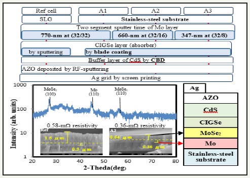
The CIGSe thin-film solar cells were fabricated on the stainlesssteel (for A1, A2 and A3 samples) and soda-lime glass (SLG, for Ref cell) substrates, respectively, and described in detail by the flowchart process of (Figure 1). In order to deposit different thickness of Mo-layer (back-electrode contact), working pressures were varied at 10 and 1m torr, separately for two-step sputtering time. The 770nm thickness of Mo layer for Ref cell and sample A1 were carried by the sputtering time of 32min (10mtorr) and 32 min (1mtorr). The thickness in sequence of sample A2 (32/16min) is 660nm and the sample A3 (32/8min) is 347nm.
Next the CIG films were deposited on the Mo layer with nonvacuum blade coating technique for to develop stainless-steel substrates, while on SLG by traditional co-evaporation processes for Ref cell. To see the effect of the CIG precursor layer, all substrates were heated with radiation at 450 ℃ on the first stage, then at 550 ℃ for selenization during the rest of stages. In the developed samples, the thickness of CIGSe layer (absorber) was deposited and controlled from 2μm to 3.9μm to absorb nearly all incidental solar light [6].
Furthermore, the non-vacuum CBD technique for buffer layer (CdS) was set up in the aqueous solution containing the thiocarbamide (SC(NH2)2), cadmium sulphate (CdSO4) and ammonium hydroxide (NH4OH). The alkaline reaction bath was prepared by using 100ml of CdSO4, 50 ml of NH4OH and 700ml of (SC(NH2)2), the CdS film deposition time is 15min at the 65 ℃ reaction temperature. Finally, fabrication of the developed CIGSe thin-film solar cell was completed by depositing of Ag (frontelectrode contact) on the 1.1μm-thick AZO film.
The X-ray diffraction (XRD, Bede D1 with Cu Kα radiation) is adjusted to the 2θ mode. A field emission gun - scanning electron microscopy (FEG-SEM, Joel, Model: JSM-6500F) is used to analyse the crystal structure of the cells. For simplification of terrestrial solar-cell characterization, the induced current density-voltage (J-V) curves of the developed devices were measured under the air mass (AM1.5) of the solar simulator (Oriel, Model: 91192) illumination at 1000W/m2 on a Keithley 2400 instrument. The sample’s external quantum efficiency (EQE) was measured by a solar cell spectral response measurement system (Enlitech, Model: QE-R).
Results and Discussion
Intrinsic stresses in Mo layers depend on the deposition working pressure, inducing significant changes in the structural and electrical properties [6]. Mo layers (illustrated as SEM images of the inset Figure 1) with 660nm thickness of A2 sample (with 0.36mΩ) has a dense and near column like microstructure with better conductivity, but the 770nm thickness of the Ref cell (with 0.58mΩ) exhibits a more open and porous structure with poor electricity.
For the identification of the Mo-Se compound on the left of the developed structure in (Figure 1), the XRD pattern indicates that the sputtered Mo layer shows a cubic crystal structure with a preferential growth orientation in (110). From the salinized Mo (MoSe2 layer), two peaks were obtained, (100) and (110), which correspond to hexagonal MoSe2 and to no other Mo-Se compound.
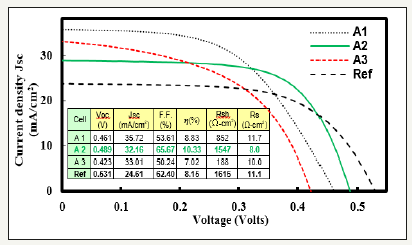
The thickness of MoSe2 layer on the Mo/substrate is revealed by the inset SEM photos, which are 1.5 and 0.54μm, respectively for the Ref cell and A2 sample. This results in decreasing the back Mo-electrode thickness from 0.77 to 0.3μm and from 0.66 to 0.36μm, separately for Ref cell and A2 sample. Figure 2 shows the J-V characteristics of the developed CIGSe thin-film solar cells with non-vacuum processes under standard conditions (AM1.5-GMM spectra, 1000W/m2 at room temperature). The main photovoltaic (PV) parameters of three samples and the Ref cell are summarized as insert table of Figure 2.
The effect of the reaction between the selenization and the Mo thickness on CIGSe cell characteristics can be realized in Figure 2. The thinner Mo layer and the higher the fill factor (F.F.) value increases the increasing the conversion efficiency (η) of CIGSe-cell performance [7]. Although sample A3 utilizes the thinnest Mo layer (347nm) for all samples, the excessive salinizing reaction suffers from the poor F.F. and η values that can be attributed to the presence of dull surface layer with a high resistivity region at the Mo/CIGSe interface [8]. This is associated with the appearance of structural and electrical properties of sputtered Mo layers as observed from Figure 1.
Figure 1:The developed Ag/AZO/CdS/CIGSe/MoSe2: Mo/flexible substrate structures of thin-film solar cells, corresponding to their experiment flow chart (on the top). The XRD pattern and SEM images (on the left) of MoSe2 layer can collate with the developed structure.

Among the processes (as detailed shown in Figure 1), sample A2 shows optimal solar-cell performance with an open-circuit voltage (VOC) of 0.489 V, short-circuit current density (JSC) of 32.16mA/ cm2, F.F.=65.67%, η=10.33%, and series resistance (RS) of 8mΩ- cm2. Furthermore, this optimal η value shows an absolute gain of 26.75% compared with the Ref cell. These improvements are the result of a reduced the MoSe2 thickness and an improved ohmic contact from the metal-semiconductor junction between a metal lead (salinized Mo layer) and CIGSe material. This results in the formation of an intermediate MoSe2 layer during CIGSe deposition [9]. From the observations above, there is a clear evidence that the formation of a MoSe2 layer is essential to facilitate a quasi-ohmic electrical contact across the CIGSe-Mo interface.
Figure 3 illustrates the spectral external quantum efficiency (EQE) in a wide-wavelength range (300-1200nm) of the developed three samples and Ref cell. It should be noted that the EQE of the developed samples are lower than those of the Ref cell for all wavelengths except for the range of 350-500nm (3.54-2.48eV). Since In-Ga interdiffusion is affected by the presence of Na with SLG substrate during CIGSe growth [10], hence, the band-gap grading is different in SLG and CIGSe absorbers, which substantial improvements of VOC, but hardly of JSC values.
In the long range of wavelengths (500-900nm), the average EQE values are 81.16%, 83.11%, 76.92%, and 76.80% for sample A1, A2, A3, and Ref cell, respectively. This indicates a clear salinizing quality improvement, which ohmic contact overcomes Na-diffusion effect on CIGSe/Mo/SLG interfaces. The A2 sample shows the most desirable average for the area under the curve (83.11%), thus it has the highest value of F.F. and the highest conversion efficiency as seen in Figure 2.
Figure 2:The current density-voltage (J-V) curves of CIGSe thin film solar cells. Performances of the developed and Ref cells are also included in bottom insert.

Figure 3:The external quantum efficiency (EQE) in a wide-wavelength range (300-1200nm) for the developed three samples and Ref cell.

Conclusion
The characteristics of the low-cost flexible CIGSe solar cells by the non-vacuum processes of three different samples were evaluated. The optimal efficiency result of 10.33% was achieved by the sample A2, which effectively yielded a gain of 26.75%abs compared with that of the Ref cell. Furthermore, the sample A2 offers features that the other solar cells lack. It has an incredibly low sheet resistance of 8.0mΩ-cm2, a filled factor of 65.67% and an average EQE of 83.11% when tested in 500-900nm range. This improved fill factor is the explanation behind the enhanced conversion efficiency of the solar cell, the film layer of MoSe2 has great ohmic contact between back electrode layer and absorber (CIGSe layer).
As shown in this paper, the non-vacuum technologies of blade coating and CBD have the characteristics of being simple, reliable, and cost efficient. These features make flexible substrate a possible standard for high-efficiency CIGSe solar cells. The high cost reductions as well as the other advantages of manufacturing thin film solar cells make this process feasible in many commercial applications.
Acknowledgment
The authors acknowledge partial support from the National Science Council of Taiwan under contract No. NSC 106-2221-E-019- 067.
References
- Pawar SM, Pawar BS, Kim JH, Joo OS, Lokhande CD (2011) Recent status of chemical bath deposited metal chalcogenide and metal oxide thin films. Current Applied Physics 11(2): 117-161.
- Wild J de, Duindam TF, Rath JK, Meijerink A, van Sark WGJHM, et al. (2013) Increased up conversion response in a-Si: H solar cells with broad-band light. IEEE J of Photovoltaics 3(1): 17-21.
- Wang SS, Ho JJ, Liou JJ, Ho JS, Hsu WC, et al. (2014) Performance improvements of selective emitters by laser openings on largearea multicrystalline si solar cells. International J of Photoenergy, pp. 1-8.
- Cheng YT, Ho JJ, Wang CK, Lee W, Lu CC, et al. (2010) Improvement of organic solar cells by flexible substrate and ITO surface treatment. Applied Surface Science 256: 7606-7611.
- JS Ho, Chang SC, JJ Ho, Hsu WT, Chiang CC, et al. (2017) Improving the performance of solar cells with novel buffer structure by the chemical bath deposition technique. Materials Science in Semiconductor Processing 59: 29-34.
- Reinhard P, Chirila A, Blosch P, Pianezzi F, Nishiwaki S (2013) Review of progress toward 20% efficiency flexible CIGS solar cells and manufacturing issues of solar modules. IEEE J of Photovoltaics 3(1):572- 580.
- Gordillo G, Grizález M, Hernández LC (1998) Structural and electrical properties of DC sputtered molybdenum films. Solar Energy Materials & Solar Cells 51(3-4): 327-337.
- Wada T, Kohara N, Nishiwaki S, Negami T (2001) Characterization of the Cu (In, Ga) Se2/Mo interface in CIGS solar cells. Thin Solid Films 387: 118-122.
- Ahn S, Kim K, Yoon K (2006) MoSe2 Formation from Selenization of Mo and Nanoparticle Derived Cu(In, Ga)Se2/Mo Films. IEEE 4th World Conference of Photovoltaic Energy Conversion 1: 506-508.
- Rudmann D, Brémaud. D, Zogg H, Tiwari AN (2005) Na incorporation into Cu (In, Ga) Se2 for high-efficiency flexible solar. J of Applied Physics 97: 1-5.
© 2018 JJ HO . This is an open access article distributed under the terms of the Creative Commons Attribution License , which permits unrestricted use, distribution, and build upon your work non-commercially.
 a Creative Commons Attribution 4.0 International License. Based on a work at www.crimsonpublishers.com.
Best viewed in


.jpg)


 Editorial Board Registrations
 Submit your Article
 Refer a Friend
 Advertise With Us
.jpg)


.jpg)


.bmp)
.jpg)
.png)
.jpg)


.jpg)


.png)

.png)


.png)


