
- About Us
- Information
-

The Author ensures that the research has been conducted responsibly and ethically with adherence to all relevant regulations. read more..
- For Authors
- For Reviewer
- Manuscript Guidelines
- Membership
- Publication Ethics
-
- Journals
- Reprints
- e-Books
- Videos
- Policies
- Contact Us
 COVID-19
- Submissions


Full Text
Research & Development in Material Science
Calculation of Carrier Distribution, Space Charge Accumulation, and Internal Electric Field Distribution in CdZnTe Detectors under Extremely High X-Ray Doses
Xiangxiang Luo, Zhuotong Du, Gangqiang Zha, Lingyan Xu and Wanqi Jie*
State Key Laboratory of Solidification Processing, China
*Corresponding author: Wanqi Jie, State Key Laboratory of Solidification Processing, and MIIT Key Laboratory of Radiation Detection Materials and Devices, China
Submission: January 23, 2019; Published: January 29, 2019

ISSN: 2576-8840 Volume9 Issue4
Abstract
We calculated the carrier density, space charge and internal electric field distribution in CdZnTe planar detectors with the consideration of four kinds of defect traps to understand its detection properties under ultrahigh X-ray flux. The results showed that severe space charge collection occurred, and the internal electric field was distorted when the X-ray flux was ultrahigh. This could strongly influence detector performance.
Keywords: Carrier distribution; X-ray detector; CdZnTe crystal
PACS:66.30.J-, 72.20.Jv, 71.55.Gs
Introduction
Photon counting CdZnTe (or Cadmium Zinc Telluride) detectors have been accepted as a new generation device for X-ray imaging in the last decades [1]. In this case, CdZnTe detector may work under extremely high X-ray dose [2-4]. For example, in medical CT, X-ray flux can be as high as 108 Photon/s/mm2 to obtain images with enough contrast [5-7]. However, CdZnTe crystal was found to have polarization effect under such high doses of X-ray [7,8]. On the other side, the amplitude of the charge signal generated by a detector can be extremely low, even at the same level of noise [9,10]. In this case, the detector will be in a “stagnation” state and cannot work properly [11-13]. Therefore, the application requires X-ray detector to possess high resolution at low X-ray dose as well as to bear high X-ray flux without deterioration. Such a task of CZT X-ray detectors is usually hindered by the existence of highdensity non-equilibrium carriers in the crystal, particularly holes with a low mobility lifetime, which are trapped by deep level defects [14-16]. The electrostatic repulsion force of the crystal defects accumulates space charge. When the accumulated space charge reaches a certain value, the electric field will be distorted, which will severely impede the transport process of carriers and deteriorate the performance of the detector [17-19]. In the present paper, the space charge accumulation behaviors and their effects on the detector performance will be evaluated by analyzing the trap and de-trap process of X-ray stimulated charges.
Methods and Calculations
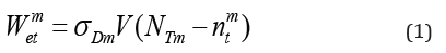
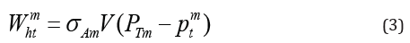
The theoretical method was proposed for the calculations of point defect effects, particularly deep-level point defects, on the space charge accumulation under extremely high doses of X-ray radiation. We used a planar detector as an example to simplify the calculation of space charge accumulation. It is assumed that EA[1~m] and ED[1~m] are the acceptor levels and donor levels in the energy band structure of CdZnTe crystal, NT[1~m] and PT[1~m] are the defect concentrations and σA[1~m] and σD[1~m] are the captured cross sections, p and n are the concentrations of holes and free electrons, and are the concentrations of the trapped electron and hole in the mth defect level, respectively. The capture rate of electrons at the mth donor level is
The de-trapping rate is
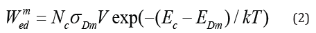
where V is the average rate of carrier thermal motion.
Corresponding to the holes, the trapping rate and de-trapping rate at the mth acceptor level are
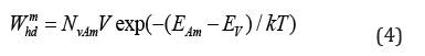
where Nv is the effective density of states in the valence band.
The incidence of the complex action of the carriers trapped at the mth defect level is
Electrons: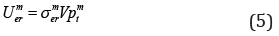
Holes:
where σmer and σmhr are the composite cross sections of electrons and holes, respectively.
Considering extremely high dose irradiation, there will be a large flux of non-equilibrium carriers in CdZnTe crystal. In this case, the probability of direct electron recombination in the conduction band and valence band will be significantly increased. R represents the unit volume per unit time. The flux is directly compounded.
where σR is the direct composite cross-section area, and n0 and p0 are the concentrations of free electrons and holes at thermal equilibrium, respectively.
It is considered that external bias is sufficiently high to neglect the diffusion motion of carriers. Based on the carrier continuity equation and the law of conservation of charge, we can derive the relationship between carrier concentration, time t, and spatial dimension Z (the external electric field along Z direction).
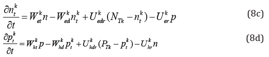
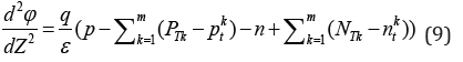
where μe and μh are the mobility of electron and hole respectively, f is the incidence of electron–hole pairs determined by the incident ray, and E is the magnitude of the electric field generated by the external bias in the crystal. From E(Z,t) = -∂φ/∂Z and Poisson’s equation, we have
The boundary conditions are
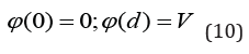
where d is the thickness of the detector and ε is the dielectric constant of CdZnTe.
We believe that X-ray energy is evenly distributed with the average value at the half of the applied voltage. According to the absorption rate of different energy rays in different CdZnTe crystals, we can determine how the rays are deposited in a crystal. The total energy generated by X-rays is
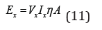
where Vx is the ray tube voltage, Ix is the tube current of the ray machine, and η is the power coefficient, which is related to the size of the tube voltage. A is the acceptance coefficient, which is related to the distance between the crystal and ray source. To solve partial differential equations (8) and (9), we use a finite element to create m CdZnTe crystal elements, as shown in Figure 1.
Figure 1:Modeling geometry of the detector.

The corresponding Poisson equation can be rewritten as
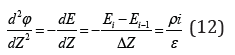
where Ei is the electric field strength at the ith and i+1th cell boundaries. It can be obtained using the boundary conditions given by equation (10).
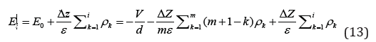
If the crystal is in an electrically neutral and thermal equilibrium state in the initial state, and the internal electric field is uniform. After time Δt, the change in the electron concentration in the ith cell caused by drift motion can be expressed as. The changes in electron concentration caused by trapping/complexing and the reverse process can be expressed as

By analogy, the change of the hole concentration in the ith cell can be obtained due to direct recombination. Based on the initial state, the space charge distribution after every time evolution of Δt can be obtained. Then, the change in the internal electric field after time Δt can be calculated. According to the changed internal electric field, the space charge distribution after the next Δt is calculated. This step is repeated until the steady state is reached.
Results and Discussion
It is assumed that the thickness of CdZnTe crystal is 2mm, the applied external voltage is 500V, X-ray is incident from the cathode sidess. μe=1000cm2/Vs, μh=100cm2/Vs and the electron–hole pair ionization energy is 4.7eV. Four representative defect levels are selected in CdZnTe crystal, as shown in Table 1.
Table 1:Defect level parameters.

Let X-ray tube voltage, tube current, and action time be 120kV, 1.00mA, and 20ms, respectively, the carrier concentration distribution is calculated with the results shown in Figure 2.
There is evidence that the trapped hole enriched in the area close to the cathode. As the distance to the anode increases, the number of enriched holes decreases, and the number of electrons increases. Positive space charge regions appear close to the cathode region. The reason on one hand, X-rays are incident from the cathode. On the other hand, owing to the relatively poor transport properties of holes, the mobility of holes is low and easy to be captured. Negative space charge distributes in a wide region and more homogeneous owing to relatively long electron transport distances. The total carrier distribution and internal electric field distribution in the crystal are shown in Figure 3.
Figure 2:Carrier density distribution (tube voltage: 120kV; tube current: 1.00mA).

Figure 3:Simulation results at the X-ray tube voltage 120KV and the tube current 1.00mA (a) distribution of electric field and (b) distribution of total carrier density.

The dotted line indicates the uniform electric field under the action of the external bias. It can be seen from Figure 3(a) that the internal electric field is significantly distorted. The electric field at the cathode has a maximum value and drops rapidly with the increase of the distance from the cathode. After a certain point, it increases again. The internal electric field determines the transit time of electrons in the crystal. The variation of the total charge density is shown in Figure 3(b). High density of the charges is generated near the cathode, which decreases with the increase of the distance. The lower density of the charges in the region away from the cathode is the sum of the native charges and those transported from the region near the cathode. To understand the charge distribution and electric field distribution in the crystal at higher doses, the X-ray tube voltage was set as 120KV and the tube current was set as 1.60mA. The results are shown in Figure 4. It is seen that the concentration of the positive space charge accumulated close to the cathode increases with X-ray dose. Accordingly, the charge concentration in the negative space charge region increases, and the distribution of the internal electric field of the crystal changes. In addition, the distortion of the internal point field is more pronounced, particularly at a distance of 0.391mm from the cathode, and zero points appear in the internal electric field. This shows that, at this point, the electrostatic force generated owing to the space charge accumulation is equivalent to the electric field force generated in the field of external power. When the electrons generated by a photon are close to the cathode, they are not only affected by the electric force of the external voltage but also by the electrostatic force of the space charge. At the zero point of the electric field, two kinds of electrons are balanced by each other. After the zero point toward the anode, the externally biased electric field force plays the dominant role and the magnitude of the internal electric field recovers gradually. Under such an electric field distribution, the transport of electrons in the crystal is more severely hindered and the transit time is considerably increased, which leads to further deterioration in the detector’s counting performance.
Figure 4:Simulation results at the X-ray tube voltage 120KV and the tube current 1.60mA (a) distribution of total carrier density and (b) inner electric field.

Figure 5:Variation in relative transit time of electrons with the depth of interaction (a) at different bias voltage, (b) at different X-ray flux.

Figure 5(a) shows the variation in the relative transit time of electrons in the crystal at different doses of lower radiation, where t’=L2/μeV, that is, the transit time under the uniform electric field generated by the external bias. The X-ray tube voltage is 120kV, and the external bias is 500V. Owing to the presence of a positive space charge region close to the cathode, the transit time of the electrons is significantly increased. The accumulated space charge concentration and the transit time of the electrons generated at the same position increase with X-ray dose. Larger transit times indicate an increased likelihood of trapping, which leads to reduced detector performance. Figure 5(b) shows the variation in the relative transit time of electrons in the crystal under different external bias voltages. Increasing external bias decreases the transit time of electrons, thereby reduces the probability of capture and recombination and improves collection efficiency. However, the leakage current and noise increase with the external voltage. Therefore, the external bias voltage is selected according to the resistivity of wafers.
Conclusion
The carrier distribution, space charge accumulation, and internal electric field distribution in CdZnTe crystals were calculated with consideration of four kinds of defect traps under extremely high X-ray doses. It was revealed that under extremely high doses of radiation, space charge accumulated in the region close to the cathode. This affected the distribution of the internal electric field and thus the performance of the detector. Electron transit time increased with X-ray dose ansssd applied bias voltage.
Acknowledgment
This work was financially supported by National Natural Science Foundations of China (Nos. 51502244, 51702271, U1631116 and 51372205), National Key Research and Development Program of China (2016YFF0101301 and 2016YFE0115200), and the fund of the State Key Laboratory of Solidification Processing in NWPU (SKLSP201741). It was also supported by the Natural Science Basic Research Plan in Shaanxi Province of China (2016KJXX-09) and the Fundamental Research Funds for the Central Universities (3102015BJ(II)ZS014).
References
- Shikhaliev PM, Fritz SG (2011) Photon counting spectral CT versus conventional CT: comparative evaluation for breast imaging application. Phys Med Biol 56(7): 1905-1930.
- Schlesinger, Toney JE, Yoon H, Lee EY (2001) Cadmium zinc telluride and its use as a nuclear radiation detector material. Materials Science & Engineering R 32(4): 103-189.
- Del SS, Leonardo A, Ezio C, Maria MA, Andrea Z, et al. (2009) Progress in the development of CdTe and CdZnTe semiconductor radiation detectors for astrophysical and medical applications. Sensors 9(5): 3491-3526.
- Abbene L, Gerardi G (2011) Performance enhancements of compound semiconductor radiation detectors using digital pulse processing techniques. Nuclear Inst & Methods in Physics Research A 654(1): 340- 348.
- Taguchi K, Iwanczyk JS (2013) Vision 20/20: Single photon counting x-ray detectors in medical imaging. Med Phys 40(10): 100901.
- Kurková D, L Judas (2016) X-ray tube spectra measurement and correction using a CdTe detector and an analytic response matrix for photon energies up to 160keV. Radiation Measurements 85: 64-72.
- Strassburg M, Schroeter C, Hackenschmied P (2011) CdTe/CZT under high flux irradiation. Journal of Instrumentation 6(1): C01055.
- Bale DS, Szeles C, (2008) Nature of polarization in wide-bandgap semiconductor detectors under high-flux irradiation: Application to semi-insulating Cd (1 – x) Zn(X)Te. Phys rev B 77(3): 035205-035205.
- Engel KJ, Herrmann C (2011) Simulation of one-dimensionally polarized x-ray semiconductor detectors. Proceedings of SPIE - The International Society for Optical Engineering 7961(2): 126-128.
- Gao W, Li X, Liu H, Hu Y, (2016) Design and performance of a 16-channel radiation-hardened low-noise front-end readout ASIC for CZT-based hard X-ray imager. Microelectronics Journal 48(C): 87-94.
- Gao W, Gan B, Li X, Wei T, Gao D, et al. (2015) Development of a compact radiation-hardened low-noise front-end readout ASIC for CZT-based hard X-ray imager. Nuclear Inst & Methods in Physics Research A 780: 15-20.
- Bale DS, Soldner SA, Szeles C (2008) A mechanism for dynamic lateral polarization in CdZnTe under high flux x-ray irradiation. Applied Physics Letters 92(8): 035205.
- Soldner SA, Bale DS, Szeles C (2007) Dynamic lateral polarization in cdznte under high flux x-ray irradiation. IEEE Transactions on Nuclear Science 54(5): 1723-1727.
- Camarda GS, Bolotnikov AE, Cui Y, Hossain A, Awadalla SA, et al. (2009) Polarization studies of cdznte detectors using synchrotron x-ray radiation. IEEE Transactions on Nuclear Science 55(6): 3725-3730.
- Pautrat JL, Francou JM, Magnea N, Molva E, Saminadayar K (1985) Donors and acceptors in tellurium compounds; The problem of doping and self-compensation. Journal of Crystal Growth 72(1): 194-204.
- Franc J, Dědič V, Rejhon M, Zázvorka J, Praus P, et al. (2015) Control of electric field in CdZnTe radiation detectors by above-bandgap light. Journal of Applied Physics 117(16): 507.
- Xu L, Jie W, Zha G, Feng T, Wang N, et al. (2014) Effects of sub-bandgap illumination on electrical properties and detector performances of CdZnTe. Applied Physics Letters 104(23): 103.
- Alekseeva L, Dorogov P, Ivanov V, Loutchanski A (2011) Investigation of the influence of light illumination on the characteristics of CdZnTe detectors. Nuclear Science Symposium and Medical Imaging Conference, pp. 4562-4566.
- Prokesch M, Szeles C (2006) Accurate measurement of electrical bulk resistivity and surface leakage of CdZnTe radiation detector crystals. Journal of Applied Physics 100(1): 103.
- Le HQ, DucoteJL, Molloi S (2010) Radiation dose reduction using a Cd ZnTe-based computed tomography system: comparison to flat-panel detectors. Med Phys 37(3): 1225-1236.
© 2019 Iman Taji . This is an open access article distributed under the terms of the Creative Commons Attribution License , which permits unrestricted use, distribution, and build upon your work non-commercially.
Editor In Chief


.jpg)


Signup for Newsletter

Quick Links
 Editorial Board Registrations
 Submit your Article
 Refer a Friend
 Advertise With Us
Our Recent Edition

.jpg)


Top Editors


.jpg)


.bmp)
.jpg)
.png)
.jpg)


.jpg)


.png)

.png)


.png)


Financial Support

Sponsors

Latest e-Books

Latest Video

 a Creative Commons Attribution 4.0 International License. Based on a work at www.crimsonpublishers.com.
Best viewed in
a Creative Commons Attribution 4.0 International License. Based on a work at www.crimsonpublishers.com.
Best viewed in