- Submissions

Full Text
Research & Development in Material Science
Ordered Defects: A Path to High-Temperature Superconductivity and Magnetic Order
Pablo DE*
Faculty of Physics and Earth Sciences, Germany
*Corresponding author: Pablo DE, Faculty of Physics and Earth Sciences, Germany
Submission: November 06, 2018; Published: November 29, 2018

ISSN: 2576-8840 Volume9 Issue1
Introduction
Defects in the atomic lattice of solids are sometimes desired. For example, atomic vacancies, single ones or more elaborated defective structures, can generate localized magnetic moments in a non-magnetic crystal lattice. Increasing their density to a few percent, magnetic order appears. Furthermore, certain interfaces can give rise to localized two-dimensional superconductivity with a broad range of critical temperatures. Old and new experimental facts emphasize the need to join e orts to start using systematically/ ordered defects” in solids to achieve room temperature superconductivity and magnetic order.
Magnetic and superconducting orders at room temperature are highly desirable due to possibilities to apply these phenomena in devices at normal life conditions, apart from the huge basic research interest. Although magnetic order is found at 300K in a not so large list of materials, superconductivity at room temperature appeared to be much more difficult to end. Here, we would like to emphasize that ordered defects in some lattice structures can provide us a path to reach both phenomena at very high temperatures in materials that do not show them in their defect free state. We would like to pay attention here on two cases of lattice defects in solids. Namely, a single or a group of vacancies and two dimensional (2D) well dined interfaces in some specific atomic lattices.
Vacancies can trigger a magnetic moment around its position in the atomic lattice. A large number of experimental and theoretical work has been done in this respect. For example, STM local measurements revealed that C-vacancies, produced by low energy ion irradiation at the surface of graphite, have a local magnetic moment [1]. Having a large enough density (5%) of hydrogen (or protons) or C-vacancies at certain positions [2,3], one can show experimentally that magnetic order at room temperature appears in graphite bulk samples. Several studies with techniques like element specific X-ray magnetic circular dichroism (XMCD) [4,5], NMR [6], magnetization and transport [7] indicate that the magnetic order triggered by defects is intrinsic and with Curie temperatures clearly above 300K. In the case of graphite [5] or ZnO [8,9], XMCD results indicate that the valence band is spin polarized in a relative large energy range, an apparently general feature in materials that show defect induced magnetism (DIM).
Due to the rather simple way to trigger in non-magnetic materials, room temperature magnetic order by low energy ion irradiation, we may ask whether some kind of devices have been already proposed. Two recent examples are worth mentioning. The rest is the spin later that occurs at the interface between magnetic and non-magnetic regions of the same material, ZnO: Li in the reported case [10]. Whereas the magnetic path of the oxide micro-or nanostructure is produced by an inexpensive 300eV proton irradiation plasma chamber, the protected nonmagnetic semiconducting regions act as a potential well for the thermally activated conduction electrons. The interfaces between magnetic and non-magnetic regions do produce a giant positive magnetoresistance, in contrast to the small and negative magnetoresistance of the magnetic paths alone. This characteristic and other details of the homo-junctions open up a new and simple way to use the spin splitting created in the irradiated oxide for spintronic devices.
Other unexpected result was obtained recently by lowenergy ion irradiation on TiO2lms. After a gentle ion irradiation hence, the originally non-magnetic lm becomes magnetic at room temperature due to Ti divacancies (which are stable at room temperature) and with the magnetization vector normal to the main area of the lm [11]. The rather large magnetic anisotropy is related apparently to the fact that the magnetic layer resides at the very near surface region. Further increase of the amount of defects by subsequent ion irradiation, vanishes the magnetic anisotropy. Recently obtained results [12] indicate that should be possible to produce nanostructured areas of TiO2 with perpendicular magnetic anisotropy. Low energy ion irradiation and the existence of DIM in several oxides may open up a new method to reach perpendicular magnetic anisotropy by far simpler and economically advantageous than several others used nowadays [13].
Let us now discuss the other order phenomenon that appears at a specially ordered lattice defect, namely at certain 2D interfaces. Systematically done STM studies of graphene bilayers showed the existence of Van Hove singularities in the electronic density of states that shift to lower bias voltages the smaller the twist angle be-tween the graphene layers [14]. As emphasized recently Figure
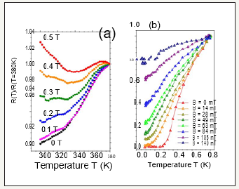
1. Normalized resistance vs. temperature at constant magnetic ends applied normal to the graphene planes and interfaces of the
Following samples:
a. Nature graphite sample; data taken from Figure 1a [14].
b. Bilayer graphene device M2 (twist angle=1:05), data taken from Figure 1b [15,16].
Figure 1:Normalized resistance vs. temperature at constant magnetic elds applied normal to the graphene planes and interfaces of the following samples:
Figure 1a: Nature graphite sample; data taken from Figure 1a [14].
Figure 1b: Bilayer graphene device M2 (twist angle=1:05), data taken from Figure 1b in [15].

By Volovik [17] the Van Hove singularities are related to the attending of the electronic energy band at well de need regions, which can be localized through the measured more pattern in the electronic spectrum. This appears to be the reason for the existence of superconductivity found recently in bilayer graphene with critical temperatures around 1K [15]. We may ask now, whether well-ordered bulk graphite samples have similar 2D interfaces. The answer is yes, indeed, and the experimental evidence is overwhelming. More patterns in the electronic spectrum measured by STM due to misoriented graphene layers of the graphite structure were found already in 1990, at the surface of a graphite HOPG bulk sample [18,19]. Their influence on the measured conductivity was not, however, realized till 2008 [20,21]. There are two more 2D interfaces that can appear parallel to the graphene planes in real graphite samples, namely:
a. The one between regions with Bernal and rhombohedral (RH) stacking orders, twisted or untwisted, and
b. Between twisted RH regions. The existence of the minority RH stacking phase was concerned in a large number of graphite bulk samples by XRD studies [14] and it’s in hence in the conductivity was recently reported [22].
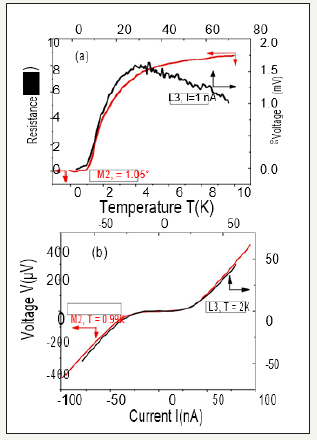
Superconductivity at these interfaces is expected to ap-pear at very high temperatures due to the existence of a dispersion less electron band, a so called at band [17]. This at band has been predicted to exist at, e.g., the surface of graphite with RH stacking order [17,23] or at the 2D interface between Bernal and RH stacking orders [24]. Its existence was concerned experimentally at the surface of small and thin RH patches surrounded by regions with Bernal stacking order [25]. It is interesting to compare the superconducting transitions identified in the temperature dependence of the Figure 2a: Temperature dependence of the resistance or voltage (at constant current) measured in the bilayer graphene device M2 (red line, taken from Figure 1b in [15], bottomleft axes) and lamella L3 (black line, taken from in [23], upperright axes). Characteristic voltage-current curves at constant temperatures obtained in the same samples shown in Figure 1a. The data of lamella L3 (black line) were taken from [23] (upperright axes) and from the bilayer graphene device (red line) from Figure 1a in [15] (bottom-left axes).
Electrical resistance at constant applied ends in a bilayer graphene [15] and the one reported two years before in several bulk samples with internal interfaces [14]. Figure 1 shows the two sets of normalized resistance data for a better comparison. As discussed in [14] the back-ground resistance in Figure 1a is simply because the volt-age electrodes do not touch the interface(s) of interest. Both transitions show some similarities worth mentioning, in spite of the two orders of magnitude difference in temperature. Namely, there is not a simple shift of the transition to lower temperatures with magnetic field, but a small applied led already prevents a complete superconducting path between the voltage electrodes. Although in the case of the bulk graphite sample Figure 1a one would tend to explain this fact by an extra magneto resistance coming from the background resistance, this does not seem to be the reason for the bilayer device.
Whereas in the case of the bulk graphite sample the transition hardly shifts to lower temperatures under an applied magnetic field (in the measured field region), the broadness of the transitions in the bilayer prevents a clear determination of a temperature dependent upper critical field Bc2(T). The overall results suggest the existence of granular superconductivity in both samples. In other words, neither in the bilayer nor in the internal interfaces of the bulk sample a homogeneous superconducting region between the voltage electrodes exists but superconducting patches. A magnetic field influences the (Josephson) coupling between those patches and there-fore no zero resistance path between the electrodes remains. In spite of granular superconductivity, at low enough fields permanent current paths can exist, the reason for us trapping [26,27] and the remnant resistance observed after removing the applied field [14]. Future studies should clarify whether the granular superconductivity is intrinsic or extrinsic due to defects (or inhomogeneous doping) at the interfaces or in the bilayer graphene. The Josephson response between superconducting patches that exist within the embedded interfaces in bulk graphite samples, can be measured by depositing electrodes directly at the edges of the interfaces, as has been done using TEM lamellae in [23].
Let us compare the results published in 2013 of one of those TEM lamellae with one of the bilayer graphene devices published recently. Figure 2a shows the temperature dependence of the resistance of device M2, see Figure 1b [15], and of the voltage (measured at constant current) of the lamella L3, see in [23]. Note rest that the transition observed in the lamella does not represent necessarily the critical temperature of the superconducting patches but the temperature where the Josephson coupling gets robust enough to influence the measured voltage. The Josephson response was identified by measuring current-voltage characteristics in both samples shown in Figure 2b at two temperatures. The Josephson characteristics curves measured in sample L3 at higher temperatures [23] are also similar to those measured in the M2 device [15] and can be very well understood following the Ambegaokar & Halperin [28] model.
Figure 2a:Temperature dependence of the resistance or voltage (at constant current) measured in the bilayer graphene device M2 (red line, taken from Figure 1b in [15], bottom-left axes) and lamella L3 (black line, taken from [23], upper-right axes).
Figure 2b: Characteristic voltage-current curves at constant temperatures obtained in the same samples shown in Figure 2a. The data of lamella L3 (black line) were taken from [23] (upper-right axes) and from the bilayer graphene device (red line) from [15] (bottom-left axes).

The clear similarities between the reported measurements in [15,23] make any further comment super uous. Future experiments should try to localize and characterize in bulk graphite samples the interfaces with higher critical temperatures in order to hopefully start their di cult but necessary production. Finally, we note that there are several examples in literature on the existence of superconductivity at 2D interfaces, apart from the interesting cases found in oxides lms [29,30]. Remarkable is the superconductivity found at the interfaces of pure Bi (a material with some similarities to graphite) and Bi Sb bi-crystals up to critical temperatures 21K [31- 34]. Moreover, dislocations at certain interfaces of semiconducting superlattices are thought to trigger superconductivity up to 6K [35,36], an idea that has been also proposed for graphite [37]. Strain induced superconductivity at interfaces of semiconducting layers has been treated theoretically based on the influence of partial at bands [38].
Acknowledgement
We are grateful to Ballestar A for discussions and a carefully reading of the manuscript. Fruitful discussions with M Stiller and J Barzola-Quiquia on their unpublished magnetic force microscopy data on TiO2 lms are gratefully acknowledge. We ac-knowledge the help of C Precker for digitalizing the data of Figure 1b.
References
- Ugeda MM, Brihuega I, Guinea F, Rodriguez JM (2010) Missing atom as a source of carbon magnetism. Phys Rev Lett 104: 096804.
- Yazyev OV (2010) Emergence of magnetism in graphene materials and nanostructures. Rep Prog Phys 73: 056501.
- Yazyev OV (2016) Theory of magnetism in graphitic materials. In: Esquinazi P (Ed.), Springer International Publishing, Switzerland, 1: 24.
- Ohldag H, Tyliszczak T, Hohne R, Spemann D, Esquinazi P, et al. (2007) Surface nucleation in the freezing of gold nanoparticles. Phys Rev Lett 98: 187204.
- Ohldag H, Esquinazi P, Arenholz E, Spemann D, Rothermel M, et al. (2010) The role of hydrogen in room-temperature ferromagnetism at graphite surfaces. New Journal of Physics 12: 123012.
- Freitas JCC, Scopel WL, Paz WS, Bernardes LV, Filho FE, et al. (2015) Determination of the hyperfine magnetic field in magnetic carbon-based materials: DFT calculations and NMR experiments. Scientific Reports 5: 14761.
- Spemann D, Esquinazi P (2016) Evidence for magnetic order in graphite from magnetization and transport measurements. In: Esquinazi P (Ed.), Basic Physics of Functionalized Graphite, Switzerland, pp. 45-76.
- Herng TS, Qi DC, Berlijn T, Yi JB, Yang KS, et al. (2010) Room-temperature ferromagnetism of cu-doped zno films probed by soft x-ray magnetic circular dichroism. Phys Rev Lett 105: 207201.
- Lorite I, Straube B, Ohldag H, Kumar P, fuerte VM, et al. (2015) Applied Physics Letters 106: 082406.
- Botsch L, Lorite I, Kumar Y, Esquinazi P, Michalsky T, et al. (2017) Spin-filter effect at the interface of magnetic/non-magnetic homojunctions in Li doped ZnO nanostructures.
- Stiller M, Barzola Quiquia J, Esquinazi P, Spemann D, Meijer J, et al. (2016) AIP Advances 6: 125009.
- Stiller M, Barzola Quiquia J. Private communication.
- Tudu B, Tiwari A (2017) Vacuum, pp. 146-329.
- Precker CE, Esquinazi PD, Champi A, Barzola Quiquia J, Zoraghi M, et al. (2016) Identification of a possible superconducting transition above room temperature in natural graphite crystals. New J Phys 18: 113041.
- Cao Y, Fatemi V, Fang S, Watanabe K, Taniguchi T, et al. (2018) Unconventional superconductivity in magic-angle graphene superlattices. Nature 556: 43-50.
- Brihuega I, Mallet P, Herrero GH, Laissardiere GT, Ugeda MM, et al. (2012) Unraveling the intrinsic and robust nature of van hove singularities in twisted bilayer graphene by scanning tunneling microscopy and theoretical analysis. Phys Rev Lett 109: 196802.
- Volovik GE (2018) Graphite, graphene and the flat band superconductivity. JETP Letters 107: 516.
- Kuwabara M, Clarke DR, Smith AA (1990) Appl Phys Lett 56: 2396.
- Miller DL, Kubista KD, Rutter GM, Ruan M, Heer WA, et al. (2010) Structural analysis of multilayer graphene via atomic moiré interferometry. Phys Rev B 81: 125427.
- Esquinazi PD, Lysogorskiy Y (2016) Experimental evidence for the existence of interfaces in graphite and their relation to the observed metallic and superconducting behavior. In: Esquinazi P (Ed.), Basic physics of functionalized graphite, Springer International Publishing, Switzerland, pp. 145-179.
- Zoraghi M, Quiquia JB, Stiller M, Esquinazi PD, Estrela Lopis I (2018) Carbon 139: 1074.
- Zoraghi M, Barzola QJ, Stiller M, Setzer A, Esquinazi P, et al. (2017) Influence of rhombohedral stacking order in the electrical resistance of bulk and mesoscopic graphite. Phys Rev B 95: 045308.
- Ballestar A, Barzola Quiquia J, Scheike T, Esquinazi P (2013) Josephsoncoupled superconducting regions embedded at the interfaces of highly oriented pyrolytic graphite. New J Phys 15: 023024.
- Kopnin NB, Heikkila TT, Volovik GE (2011) High-temperature surface superconductivity in topological flat-band systems. Phys Rev B 83: 220503.
- Munoz WA, Covaci L, Peeters F (2013) Tight-binding description of intrinsic superconducting correlations in multilayer graphene. Phys Rev B 87: 134509.
- Pierucci D, Sediri H, Hajlaoui M, Girard JC, Brumme T, et al. (2015) Evidence for flat bands near the fermi level in epitaxial rhombohedral multilayer graphene. ACS Nano 9: 5432-5439.
- Stiller M, Esquinazi PD, Quiquia JB, Precker CE (2018) J Low Temp Phys pp. 191-105.
- Ambegaokar V, Halperin BI (1969) Voltage due to thermal noise in the dc Josephson effect. Phys Rev Lett 22: 1364.
- Mohanta N, Taraphder A (2014) Phase segregation of superconductivity and ferromagnetism at the LaAlO3/SrTiO3 interface. J Phys Condens Matter 26(2): 025705.
- Boschker H, Manske D, Mannhart J (2016) Physik Journal pp. 15-37.
- Gitsu DV, Grozav AF, Kistol VG, Leporda LI, Muntyanu FM (1992) Experimental observation of a superconducting phase with Tc~- 8.5K in large-angle bismuth bicrystals. JETP Lett 55: 403.
- Muntyanu FM, Leporda LI (1995) Phys Solid State 37: 298.
- Muntyanu FM, Gilewski A, Nenkov K, Zaleski AJ, Chistol V (2007) Fermisurface rearrangement in Bi bicrystals with twisting superconducting crystallite interfaces. Phys Rev B 76: 014532.
- Muntyanua F, Gilewski A, Nenkov K, Zaleski A, Chistol V (2008) Solid State Communication pp. 147-183.
- Fogel NY, Pokhila AS, Bomze YV, Sipatov AY, Fedorenko I, et al. (2001) Novel superconducting semiconducting superlattices: dislocationinduced superconductivity? Phys Rev Lett 86: 512.
- Fogel NY, Buchstab EI, Bomze YV, Yuzephovich OI, Mikhailov MY, et al. (2006) Direct evidence for interfacial superconductivity in two-layer semiconducting heterostructures. Phys Rev B 73: 161306.
- Esquinazi P, Heikkila TT, Lysogoskiy YV, Tayurskii DA, Volovik GE (2014) On the superconductivity of graphite interfaces. JETP Letters 100: 336- 339.
- Tang E, Fu L (2014) Strain-induced partially flat band, helical snake states and interface superconductivity in topological crystalline insulators. Nature Physics 10: 964-969.
© 2018 Pablo DE. This is an open access article distributed under the terms of the Creative Commons Attribution License , which permits unrestricted use, distribution, and build upon your work non-commercially.
 a Creative Commons Attribution 4.0 International License. Based on a work at www.crimsonpublishers.com.
Best viewed in


.jpg)


 Editorial Board Registrations
 Submit your Article
 Refer a Friend
 Advertise With Us
.jpg)


.jpg)


.bmp)
.jpg)
.png)
.jpg)


.jpg)


.png)

.png)


.png)


