- Submissions

Full Text
Research & Development in Material Science
Present and Future Nanoelectronics Devices-An Analytical Study
Dalvinder Singh Grewal*
Department of English, Guru Nanak Dev Engineering College, India
*Corresponding author: Dalvinder Singh Grewal, Department of English, Guru Nanak Dev Engineering College, Ludhiana, India
Submission: October 26, 2018; Published: October 30, 2018
ISSN: 2576-8840 Volume8 Issue4
Applications of Nanoelectronics
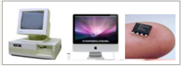
Nanoelectronics is a wing of nanotechnology that deals with the integration of purely electronic devices, electronic chips and circuits at miniaturised scale. Analogue/ RF circuits combine to make the digital systems. Domain of development has now reached ‘More than Moore’. A memory chip or a package of nanoelectronic components measured on the nanoscale dimensions for systems has the giga-scale complexity (Figure 1).
Figure 1:Nanoelectronics in computers and digital displays.

Nanotechnology has created wonders in electronics by reducing the size of transistors used in ICs. A memory chip with a projected density of 1 terabyte of memory per square inch is now under development. This increases the density of memory chips. Display screens on electronics devices are improved, reducing power consumption and weight and thickness of the screens. It has helped nanoelectronics to cross traditional scaling limits in standard CMOS technology. These nanoelectronic components are called ‘Beyond CMOS’ domain of development.
In giga systems, the number of components in a system may reach gigascale orders when systems are designed using nanoscale components thereby increasing number of challenges like complexity in scaling up to gigascale. Scaling of electrical properties likes power dissipation, supply voltage, speed, and leakage currents by nanotechnology has directed electronic power designs in new architecture. Development of new components for electronic system design with a fusion of nanotechnology is revolutionary. To block UV radiation many sun screens use nano-sized particles of titanium dioxide and zinc oxide effectively (Figure 2)
Figure 2:Nanotechnologies in electronics.
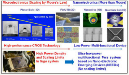
Figure 3:Nano integrated circuits.
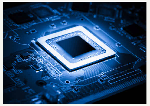
The phenomenal growth in the CMOS technology over the past four decades is due to high performance and storage systems. Planar CMOS technology is the main component for embedded electronic systems design from several decades. It has been scaled according to Moor’s law resulting in ever decreasing device sizes and in a number of technology nodes, the present one being the 14nm node and in general, the scaling cannot go below approximately 10nm for MOS transistors. High-performance logic circuits and semiconductor memory had been the technology drivers to architect the miniaturisation of the MOS transistor. The scaling of the MOS transistor in nanoelectronics explores new materials like high-k gate dielectrics such as HfO2, Er2O3, Gd2O3; new channel materials such as germanium and graphene and finally new device structures like double-gate FET, FinFET and Schottky source/drain FET (Figure 3)
Industrial and Global Implications
Light and smart products are both easy to carry and provide accuracy and quality. Power requirement is reduced. This has helped increase the world market which now is going to cross trillion dollars. Presently Samsung, IBM, Apple, Intel, Lenovo, LG electronics, AMD, Eikos, IOGEAR, a123systems, Starkey, Multiple Manufacturers and other organisations are using nanoelectronics in their manufacturing systems extensively. Industry employs nanotechnology experts as engineers, managers, controllers, technicians and assistants. Products are easy to carry or move as these are very light. The power requirement too has been reduced. Electronic components are now practically made with the NEMS related to the MEMS. The new well-developed and less costly products include computer hardware, display devices, mobile and communication products, audio products, camera and films. In progress are the production of SETs and controlled electron tunnelling to amplify current, resonance tunnelling device and current controlled quantum device for further research [1-11].
Current trends in nano electronics:
1. Development of new applications
2. Miniaturisation of existing ones
3. Ideas for new emerging fields
4. Molecular electronics made as the base.
5. Self-assembled monolayer (SAM) (an organised layer of amphilic molecules).
Nanoelectronics for Wireless Devices
Ambient intelligence, where, computation and communication is always available and ready to serve the user in an intelligent manner remains the vision of the wireless industry which the current technologies cannot resolve. The solution lies in nanotechnology which is capable of providing solutions through new technologies. New material and new sensing elements for sensors will be enabled by nanotechnology which will have applications in industries like transportation, communication, building and facilities and in military operations ensuring safety and internal and external national security. Future nanotechnology will help in increasing the memory storage capacity to a phenomenal level by new inventions since more memory will be required in computers, mobile phones and elecrtronics-based machinery.
Future of nanoelectronics
1. Future of mobile electronics lies in stretchable or flexible electronics.
2. The potential applications may include wearable electronic devices, biomedical uses, compact portable devices and robotic devices.
3. Graphene, an allotrope of carbon, is likely to become a dominant material in flexible electronics in future. Because of its superb electrical conductivity, flexibility and physical strength it will replace other carbon products in the Nano field.
Research in progress
Nanoelectronics applications on the research tables include the following (Figure 4):
Figure 4:Applications of nanoelectronics under development.

A. For low power requirements, simple fabrication process and combination of flexibility research is being conducted on cadmium selenide nanocrystals deposited on plastic sheets to form flexible electronic circuits.
B. CMOS integrated circuits to have integrated silicon nanophotonics components, for higher speed data transmission between ICs than is possible with electrical signals.
C. To use nanomagnets as switches, like transistors, in electrical circuits Berkeley scientists demonstrated a low power method which might lead to electrical circuits with much lower power consumption than transistor based circuits.
D. To form the conductive lines needed in circuit boards silver nanoparticle ink was used. Scientists at Tokyo University developed a method to print prototype circuit boards using standard inkjet printers.
E. Developing a lead free solder reliable enough for space missions and other high stress environments using copper nanoparticles.
F. Functioning integrated circuits using carbon nanotubes have been developed by researchers at Stanford University. They had also developed methods to remove metallic nanotubes, an algorithm to deal with misaligned nanotubes.
G. Laser that uses a nano-patterned silicon surface that helps produce the light with much tighter frequency control was developed by researchers at Caltech.
H. Nanowires made from electrodes would enable flat panel displays to be flexible.
I. Transistors built using single atom thick graphene film to enable very high speed transistors.
J. Building transistors from carbon nanotubes to enable minimum transistor dimensions of a few nanometres and developing techniques to manufacture integrated circuits built with nanotube transistors.
K. PN junctions, a key component of transistors have been developed from graphene.
L. Combining gold nanoparticles with organic molecules to create a transistor known as a NOMFET (Nanoparticle Organic Memory Field-Effect Transistor).
M. Making integrated circuits with features that can be measured in nanometres (nm)
N. Using carbon nanotubes to direct electrons to illuminate pixels, resulting in a lightweight, millimetre thick ‘nanoemmissive’ display panel.
O. Using nano-sized magnetic rings to make magnetoresistive random access memory (MRAM).
P. Researchers have developed a lower power, higher density method using nanoscale magnets called magnetoelectric random access memory (MeRAM) and also developed molecular-sized transistors that increase transistor density in integrated circuits.
Q. Using self-aligning nanostructures to manufacture nanoscale integrated circuits.
R. Using nanowires to build transistors without p-n junctions, bucky balls to build dense, low power memory devices, magnetic quantum dots, silver nanowires embedded in a polymer to make conductive layers without damaging the conductor, nanowires made of an alloy of iron and nickel to create dense memory devices.
S. Memory chip that uses carbon nanotubes developed by IMEC and Nantero. This memory is known as NRAM for nanotube-based non-volatile random-access memory. Future applications at the nanoscale will include treating cancer, generating renewable energy and providing clean water anytime, anyplace. The greatest challenge to benefiting from nanotechnology is having the foresight to develop and use it wisely (Table 1).
Table 1:Projects under research.

Eliminating internal problems
The heat produced by integrated circuits and consumption of power are the problems that are faced by both laptop users and highperformance data centres. The researchers are exploring new way for designing and making logic circuits by integrating photosensitive organic molecules into tiny particles of semiconductor material called quantum dots.
Needed Motivation in Nano Research
Conventional CMO technology device physics scaling and interconnects are limited to negative resistance devices switches, spin transistors, single electron transistor devices and circuits and quantum cellular automata (QCA). Quantum computing, quantum information processing (QIP), sensing and biological interface and self-assembly and biometric behaviours can be the new information processing paradigms and a new alternative in nanoelectronics. Smaller dimensions increase sensitivity to fluctuations; manufacturability and reproducibility and limited demonstration system, however, performance improves with these decreased dimensions. This remains an important issue. Motivation in research in nanoelectronics can come from all these limits and new alternatives can become available.
With the advancement of technology, the energy consumption of CMOs has improved continuously by reducing the supply voltage. The increasing requirement of portability requires further energy consumption and long life of the battery cells. Several device technologies and circuit styles have constantly attended to higher performance and low standby leakage. The use of multiple and variable threshold CMOS, dual-gated SOI technology and backgate effect have left a visible impact on the nanoelectronic field development. The dynamic control of threshold voltages is being achieved in triple-well CMOS. These technologies reduce leakage power during idle periods and enable low-threshold, high-speed operations during active periods.
Suggested Direction for Future Research:
1. Sensors, actuators, displays, imagers, fluidic or biointerfaces (DNA, Protein, Lab-on-chip and Neuron interfaces) are going to be interfacing the real world. These are the specific transducers that are based on the non-electrical phenomenon to create interaction.
2. New devices are needed for enhancing electronics with nonpure electrical devices in signal processing and RF or analogue circuits. Regular MOS circuits do not achieve certain transfer functions due to electrical characteristics and need better system performances. In this category fall the RF MEMS electro-acoustic high qulity resonators.
3. Autonomous sensors or circuits with permanent active security monitoring with embedded power sources having onchip or in-package micro power sources in electronics will have several new applications. Energy scavenging micro batteries are examples of this category (Figure 5).
Figure 5:Changing computer structure.
Suggested ways for future improvement:
1. Increasing the number of transistors and circuits per chip.
2. Reduction in size, weight, mass as well as power consumption.
3. Continuous improvement in electronic devices and display.
4. Density increase in memory chips.
Conclusion
Electronics works at the atomic scale for developing nanomachines targeting size, surface and volume reduction of materials. Accurate treatment at atomic and molecule levels undergoes long processes of manufacturing. For fabrication of silicon based devices, top down approaches are dominating the electronic industry so far,. Nanoscale NEMS, MEMS, microprocessors, optical switching and other electronic components will play an important part in future production in electronics. Scaling up to CMOs will be improvised and replaced by deposition, implantation, lithography and metrology.
The promising nanostructure in nanoelectronics provides a great variety of interest. Once process compatibility is proven, integration with CMOs will be the first step in the profitable use of nanostructure. Reliability, stability and lifetime and other critical issues will become routine. These will then be addressed at a circuit/ architecture level. For the full exploitation of nanocomputers, novel circuits and architectures will be needed. The new promise of the future nanoelectronics is the development and enhancement of mobile devices and portable, flexible, stretchable and wearable devices. Miniaturisation of ICs by applying nano electronics has a great promise. Design and functionality for the devices requires a new approach with the flexibility in the world of electronics. Additional dimension of flexibility is now available to electronics manufacturers and a huge change brought by it will make its impact into the commercial realm.
References
- Daniel Burrus (2013) Dematerialization-A pathway for innovation. Huffpost.
- www.bfi.org/gbn_ecology.pdf
- http://www.steel.org/media/
- http://phe.rockefeller.edu/dematerialization/
- http://www.memagazine.org/contents/current/features/frontier/ frontier.html
- http://future.sri.com/Explorer/NT.shtml
- Dalvinder SG (2014) Saving space from buildings by nanotechnology. IOSRJEN 4(2): 39-48
- Dalvinder SG (2015) Super strong nano-composite materials for bunkers & command posts. Army Nanotechnology Congress & Expo,Frankfurt, Germany.
- Roco MC (2013) Scientists are building the next generation of atomicscale devices, Atomic Toolbox: Manufacturing at the Nanoscale, Scientific American, USA.
- Farhad Nabhani (2009) Proceedings of the 19th International conference on flexible automation and intelligent manufacturing. FAIM, Teesside University, Middlesbrough, UK.
- Penn IT (2001) Web-based survey of trends in dematerialization, Report No. CSS01-17, A report of the Center for Sustainable Systems, Center for Sustainable Systems, University of Michigan, USA.
© 2018 Dalvinder Singh Grewal . This is an open access article distributed under the terms of the Creative Commons Attribution License , which permits unrestricted use, distribution, and build upon your work non-commercially.
 a Creative Commons Attribution 4.0 International License. Based on a work at www.crimsonpublishers.com.
Best viewed in


.jpg)


 Editorial Board Registrations
 Submit your Article
 Refer a Friend
 Advertise With Us
.jpg)


.jpg)


.bmp)
.jpg)
.png)
.jpg)


.jpg)


.png)

.png)


.png)


