
- About Us
- Information
-

The Author ensures that the research has been conducted responsibly and ethically with adherence to all relevant regulations. read more..
- For Authors
- For Reviewer
- Manuscript Guidelines
- Membership
- Publication Ethics
-
- Journals
- Reprints
- e-Books
- Videos
- Policies
- Contact Us
 COVID-19
- Submissions


Full Text
Research & Development in Material Science
Piezoelectric,Optical and Electrical Characterization of Vertical ZnO Nanowires
Marwa Bakour1*,Batal M A1 and Amir AlhajSakur2
1 Department of Physics, Aleppo University, Syria
2 Analytical and Food Chemistry Department, Aleppo University,Syria
*Corresponding author: MarwaBakour, Department of Physics, Aleppo University,Aleppo, Syria
Submission: April 01, 2018; Published: July 02, 2018

ISSN: 2576-8840 Volume6 Issue5
Abstract
Oxide nanowire arrays were studied for piezoelectric applications.Such as ZnO nanowire arrays growth on silicon substrate. The effects of thermal annealing on the optical properties of ZnO nanowires were prepared on sol-gel ZnO-seed-coated substrates. AFM images were found at 130°C well aligned vertically, and the well defined crystallographic planes, providing strong evidence that the nanowire arrays orientate along the c-axis. The annealing temperature of the ZnO thin film plays an important role on the microstructure of the ZnO grains and then the growth of the ZnO nanowire arrays. From PL spectra, an evident ultraviolet near-band edge emission peak at 382nm is observed.From (I-V) characteristic that the material behaves p-n junction diode, ideality factors >>2.0, that was attributed to tunnelling via deep levels in the forbidden gap. Impedance spectra shows the spectrum of the Impedance resistance that the curve does not represent a regular semicircle andthis indicates that the structure of the material is not regulated granules but rather is in a different form which is the nanowires. From Piezoelectric characterization, voltage increase with increase the force applied on Nanowires.
Keywords: C-axis ZnO nanowires; ZnO seed layer; Sol-Gel;AFM images; PL spectra; (I-V) characteristics; Ideal factor;Impedance spectra;Piezoelectric characterization
Introduction
Figure 1:Hexagonal wurtzite structure of ZnO.

In recent years, zinc oxide (ZnO) has attracted a lot of attention because of its interesting physical properties such as its wide and direct band gap (3.37eV), large exciton binding energy (60meV), high electron mobility, and high thermal conductivity [1], exhibiting near UV light emission, transparent conductivity, hexagonal crystal structure (Figure 1). These features render ZnO suitable for several applications ranging from optoelectronics [2], piezoelectric and photovoltaic systems [3]. In this research we try to find a way to convert mechanical energy into electric power with the use of aligned zinc oxide (ZnO) nano wires. The mechanism of the power generator relies on the coupling of piezoelectric and semiconducting properties of ZnO as well as the formation of a Schottky barrier between the metal and ZnO contacts. One-dimensional ZnO nanostructures such as nano wires have been extensively studied for other applications including solar cells [4], ultraviolet (UV) light-emitting diodes [5], photonic crystals and transparent electrodes [6]. Several methods have been demonstrated to fabricate one-dimensional ZnO nanostructures, such as vapour liquid solid epitaxial (VLSE), chemical vapour deposition (CVD) [7]. However, the high temperatures required for these gas deposition techniques (above 5000C for CVD and 9000Cfor VLSE) and pulse laser deposition (PLD) [8], but these techniques still have some limitations for substrate size and the need for high temperature operation.
Recently, the growth of ZnO nano wires in phase solutions at low temperature (below 100 °C) was reported by using the hydrothermal process, the growth had been on glass, silicon wafer and plastic substrates [9]. This method shows that the shape of the ZnO nano wires was sensitive to the orientation of Si substrate via the use of ZnO nano particles as a seed layer. However, systematic research on the influence of quality characteristics of ZnO sol-gel thin films on the growth of ZnO nano wire arrays via hydrothermal method has rarely been reported. In this work, now catalytic method and ZnO, cost effective, non-catalytic method and ZnO sol-gel thin films were used as the seed layers with different temperatures annealing.
Experimental details
Upturned crystalline growth method is two phases:
A. Preparation seed layer thin films: The ZnO thin films served as the seed layers were deposited on silicon substrates by a sol-gel method [10]. A coating solution contained zinc acetate dehydrate (Zn (CH3COO)22H2O, Merck, 99.5% purity) and equivalent molar mono ethanolamine (MEA) (NH2 CH2CH2OH, Merck, 99.5% purity) dissolved in 2-methoxyethanol (2MOE) (CH3OCH2CH2OH, Merck, 99.5% purity). The concentration of zinc acetate was chosen to be 0.5mol/L. The resulting solution was then stirred at 60 °C for 2h to yield a homogeneous solution, which served as the coating solution after being cooled to room temperature. Then the solution was coated onto p-type silicon (111) substrates by a spin coater at the rate of 1000rpm for 30s at room temperature. Subsequently, the films were preheated for 10min to remove the residual solvent. Then the layer film was annealed in a furnace at different temperatures ranging from 130 to 900 °C for 2h.
B. Growth Vertical ZnO Nano wires arrays: After uniformly coating the silicon substrates with ZnO thin films, growth of ZnO nano wire arrays was achieved by suspending these ZnO seed-coated substrates upside down in a glass beaker filled with solution of 50mM zinc nitrate hexa hydrate (Zn(NO3)2·6H2O, 98% purity) and 50mM hexamethylenetetramine (HMT) (C6H12N4, 99.5% purity). During the growth, the glass beaker was heated with a laboratory oven maintained at 60 °C for 12h. At the end of the growth period, the substrates were removed from the solution, then immediately rinsed with de-ionized water to remove any residual salt from the surface, and dried in air at room temperature.
Results and Discussion
Surface morphologies (AFM Images)
Figure 2 shows the AFM images for the surface morphologies of ZnO nano wire arrays at different annealing temperatures of the thin films. It is notable that the ZnO nano wire arrays on the ZnO thin films annealed at 130 °C are well aligned vertically (Figure 2a), and the well defined crystallographic planes, providing a strong evidence that the nano wire arrays orientate along the c-axis. This implies its perfect c-axis orientation. As the annealing temperatures of the ZnO thin films increase from 130 to 900 °C, the diameters of the ZnO nano wire arrays increase from 10 to 80nm in average and its high ranging from 300 to 400nm. The reason may be that the high annealing temperature evidently increase the interaction among the grains and leads the grains to merge together to form bigger ZnO seeds, and thus increases the diameter of the ZnO nano wires Figure 2b-2d.
Figure 2:
AFM images of ZnO after growth nanowires arrays (seed layer anneling at different temperature
2a: t=130 °C;
2b: t=300 °C;
2c: t=600 °C;
2d: t=900 °C.

Electrical properties
Figure 3:I-V characteristics of Nanowires ZnO that seed layer annealing at 130 0C.

Figure 4:I-V characteristics of Nanowires ZnO that seed layer annealing at 300 0C.

Figure 5:I-V characteristics of Nanowires ZnO that seed layer annealing at 600 0C.

(I-V) Curves for ZnO Nano wire arrays: I-V characteristics of Nano wires ZnO arrays measured at room temperature are shown in Figure 3-7. Figure 3-7 shows that at constant voltage, the current value of the voltage is increase than its value in case of voltage decrease there is a slow loop. This is due to the fact that while lifting the applied voltage, the ions on the trap level have moved to another more closely related crystalline structure leading to decreasing charge carriers during the decrease in applied voltage and thus the current decline. Note from the (I-V) characteristic that the material behaves p-n junction diode. As per the Sah-Noyce- Shockley theory [11], the forward current in a p-n junction is dominated by recombination of minority carriers injected into the neutral regions of the junction. This type of current gives an ideality factor of 1.0. Recombination of carriers in the space charge region, mediated by recombination centers located near the intrinsic Fermi level, results in an ideality factor of 2.0 [12]. The high ideality factors (n>>2.0) in LEDs or p-n junction diode were attributed to deeplevel- assisted tunneling, due to temperature-independent slopes of (log I)-versus-V plots. Ideality factors close to 2.0 were attributed to space charge region recombination, consistent with the Sah-Noyce- Shockley theory, due to temperature-dependent slopes of (log I)-versus-V plots. However, a comprehensive theory for the high ideality factors found experimentally in p-n junctions has not been presented. The ideal factor can be calculated by drawing the graph of Ln(I) with V as in Figure 8.
Figure 6:I-V characteristics of nanowires ZnO that seed layer annealing at 900 0C.

Figure 7:Schematic representation of I-V characteristics and carrier transport mechanism for diode ideality factors of n=1.0 and n=2.0.

Figure 8:(Ln (I)-V) in the forward bias voltage range at voltage rise.

The ideal factor of the equation (1) can be calculated:
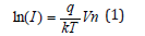
Where q is the elementary charge, k is the Boltzmann constant, T is the absolute temperature, and n is the ideality factor. Where attention is given to the linear area of the curve [13]. The ideal factor values were arranged in Table 1 it is apparent that ideality factors >>2.0 can be measured, that was attributed to tunneling via deep levels in the forbidden gap.
Table 1: Ideal factor values

Impedance spectra measurements: Using a gain phase analyzer devise type (Schlumberger-SI1253) with detection resistance Rd. A variable frequency signal [0.1Hz-20KHz] was applied to the material and a fixed input voltage (V1=5v) was applied. To determine the spectrum of impedance spectra, the equation (2) can be used:
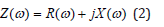
Table 2: Deceleration time values at different annealing temperature.

Figure 9 shows the curves are regular semicircles. So the structure of the granular material in the seed layer represents the equivalent circuit between the granules is intense and connected in parallel with the resistance. Figure 10 shows the spectrum of the Impedance resistance that the curve does not represent a regular semicircle and this indicates that the structure of the material is not regulated granules but rather is in a different form which is the nano wires [14]. The time of deceleration (τ) of the electron can be determined by drawing the real section of the impedance with frequency as shown in Figure 11. Since the deceleration time is equal to the inverted frequency at the top of the curve (Table 2).
τ = ω1 = 21π
Figure 9:Impedance spectra scope of ZnO Seed layer deposits on p-Si.

Figure 10:Impedance spectra scope of ZnO nanowires arrays growth on p-Si.

Figure 11:The real section of Impedance with Frequency of ZnO nanowires arrays growth on p-Si.

Piezoelectric characterization
Various forces were applied to a very small area of the vertical Nano wires ZnO surface. In contrast, the voltage obtained by applying force on the sample was measured by Nano voltage meter device in order to study the piezoelectric properties. Figure 12 & 13 shows that the voltage increases with the intensity of the force applied vertically to the nano wires, indicating that the material has the piezoelectric characteristics.
Figure 12:The force applied on ZnO nanowires and voltage measurement

Figure 13:Piezoelectric characterization of ZnO nanowires at different temperatures.

References
- Zhong LW (2004) Nanostructures of zinc oxide. Materials Today 7(6): 26-33.
- Duan X, Huang Y, Cui Y, Wang J, Lieber CM (2001) Indium phosphide nanowires as building blocks for nanoscale electronic and optoelectronic devices. Nature 409(6816): 66-69.
- Ozgur YI, Alivov C, Liu A, Teke MA, Reshchikov S, et al. (2005) Growth of ZnO nanolayers inside the capillaries of photonic crystal fibre. J Appl Phys 98: 041301.
- Law M, Greene LE, Johnson JC, Saykally R, Yang PD (2005) Nanowire dyesensitized solar cell. Nature Materials 4: 455-459.
- Lim JH, Kang CK, Kim KK, Park IK, Hwang DK, et al. (2006) UV electroluminescence emission from ZnO eight-Emitting diodes grown by high temperature radiofrequency sputtering. Adv Mater 18(20): 2720- 2724.https://onlinelibrary.wiley.com/doi/abs/10.1002/adma.200502633
- Znaidia L, Touamb T, Vrela D, Soudeda N, Yahiaa SB, et al. (2012) ZnO thin films synthesized by sol-gel process for photonic applications. Acta Physica Polonica A 121(1): 165-168.
- Ikegami K, Yoshiyama T, Maejima K, Shibata H, Tampo H, et al. (2009) Optical dielectric constant inhomogeneity along the growth axis in ZnObased transparent electrodes deposited on glass substrates. J Appl Phys 105: 093713-093719.
- Wu JJ, Liu SC (2002) Low-temperature growth of well-aligned ZnO nanorods by chemical vapor deposition. Adv Mater 14(3): 215-218.
- Varanasi CV, Leedy KD, Tomich DH, Subramanyam G, Look DC (2009) Improved photoluminescence of vertically aligned ZnO nanorods grown on BaSrTiO3 by pulsed laser deposition. Nanotechnology 20: 38.
- Yong Q, Rusen Y, Zhong LW (2008) Growth of horizonatal zno nanowire arrays on any substrate. J Phys Chem C 112 (48): 18734-18736.
- Shuxi D, Yang W, Dianbo Z, Xiao H, Qing S, et al. (2011) Fabrication of surface-patterned ZnO thin films using sol-gel methods and nanoimprint lithography. Journal of Sol-Gel Science and Technology 60: 17.
- Tanvir A, Sharmin S, Faysal NM (2016) Comparative analysis between single diode and double diode model of PV cell: concentrate different parameters effect on its efficiency. Journal of Power and Energy Engineering 4(3): 31-46.
- Jay MS, Li YL, Gessmann T, Schubert EF (2003) Experimental analysis and theoretical model for anomalously high ideality factors (n>>2.0) in AlGaN/GaN p-n junction diodes. Journal of Applied Physics 94(4): 2627- 2630.
- Abdullah K, Bui A, Loubierre A (1991) Low frequency and low temperature behavior of ZnO-based varistor by ac impedance measurements. Journal of applied phys 69(7): 4046-4052.
© 2018 Marwa Bakour . This is an open access article distributed under the terms of the Creative Commons Attribution License , which permits unrestricted use, distribution, and build upon your work non-commercially.
Editor In Chief


.jpg)


Signup for Newsletter

Quick Links
 Editorial Board Registrations
 Submit your Article
 Refer a Friend
 Advertise With Us
Our Recent Edition

.jpg)


Top Editors


.jpg)


.bmp)
.jpg)
.png)
.jpg)


.jpg)


.png)

.png)


.png)


Financial Support

Sponsors

Latest e-Books

Latest Video

 a Creative Commons Attribution 4.0 International License. Based on a work at www.crimsonpublishers.com.
Best viewed in
a Creative Commons Attribution 4.0 International License. Based on a work at www.crimsonpublishers.com.
Best viewed in