- Submissions

Full Text
Polymer Science: Peer Review Journal
Solvent Vapor Annealing of Perovskite Films for High Performance Perovskite Solar Cells: A Mini-Review
Mohamed I Omer1,2, Wang Xizu2 and Tang Xiaohong1*
1Center for Optoelectronics and Bio photonics, School of Electrical & Electronic Engineering, Nanyang Technological University, Singapore
2Institute of Materials Research and Engineering (IMRE), Agency for Science, Technology and Research, Singapore
*Corresponding author: Tang Xiaohong, Center for Optoelectronics and Bio photonics, School of Electrical & Electronic Engineering, Nanyang Technological University, Singapore
Submission: March 23, 2022;Published: April 13, 2022

ISSN: 2770-6613 Volume3 Issue3
Abstract
Perovskite Solar Cells (PSCs) have undergone a rapid development and progress in recent years, achieved high power conversion efficiencies beyond 20%. This was made possible through the developments in different areas of the device and its process engineering, including the development of PSCs interface interfacial engineering techniques. In addition to the modification of the perovskite absorber layer by means of additives, solution engineering and various post-treatments of the perovskite layer such as Solvent Vapor Annealing (SVA) have also been developed and applied for developing high performance PSCs. This short review reviews the recent advancements in SVA post-treatments of perovskite films to modify and tune their grain morphology, crystallinity and trap density, and thereby improving the PSCs performance and stability.
Keywords:Perovskite solar cells; Crystallinity; Photoluminescence; Solvents; Photocurrent
Abbreviations: PSCs: Perovskite Solar Cells; SVA: Solvent Vapor Annealing; DMF: Dimethylformamide; GBL: Gamma-Butyrolactone; DMSO: Dimethyl-Sulfoxide; NMP: N-Methyl-2-pyrrolidone
Introduction
In Perovskite Solar Cells (PSCs), the properties of the perovskite absorber layer, particularly its grain morphology, crystallinity and trap density, are of critical importance for the device performance and stability. Since the early days of PSCs research, a special attention has been paid to improving the perovskite film morphology by various means, including solution engineering [1-3] and optimizing the film deposition procedures and conditions [4-9]. Later on, Solvent Vapor Annealing (SVA) becomes a very effective method that can drastically modify the perovskite film’s grain morphology, in addition to its crystallinity, leading to an improvement in the overall PSC efficiency. SVA post-treatment is generally based on keeping the as-deposited perovskite film under atmospheric conditions with an elevated concentration of a solvent vapor for a period of time during thermal annealing. Under such conditions, the solvent vapor (typically a polar solvent that dissolves the perovskite precursors) would mediate the growth of large grains through Ostwald ripening process [10,11], in which the smaller grains in the film are melted and re-deposited as the larger ones, therefore leading to a morphology that is more favorable for the performance of PSCs. The following sections summarize the SVA of perovskite films to achieve high performance of PSCs, including the utilized solvents or solvent mixtures, and the key changes observed in the film’s characteristics and PSCs performance.
SVA using Single Solvents
The first report on utilizing SVA in the preparation of perovskite films was made by Xiao et al. [12] in which they used Dimethylformamide (DMF) as a solvent to treat perovskite films that are deposited through a two-step method (i.e., depositing PbI2 films first followed by immersion into MAI solution to complete the conversion to perovskite). They reported a significant increase in the perovskite grain size, reaching up to 1μm compared to 260nm for the control films. Additionally, an increase in the film’s crystallinity was confirmed by XRD analysis. Overall, these modifications resulted in an increased carrier recombination lifetimes and a faster extraction as confirmed by transient photovoltage and photocurrent measurements. This resulted in the PSCs with a PCE of 15.6% as compared to only 9.9% for the control devices [12]. Subsequently, a work by Jiang et al. [13] evaluated the impact of five different annealing atmospheres, N2, H2O, Gamma- Butyrolactone (GBL), Dimethyl-Sulfoxide (DMSO), and DMF, on the perovskite film’s characteristics N2, H2O, Gamma-Butyrolactone (GBL), Dimethyl-Sulfoxide (DMSO), and DMF. A notable change in the morphology and an increase in crystallinity of the perovskite films was observed when it was annealed in DMF, GBL and DMSO ambient. While H2O annealing ambient showed no beneficial effects on the perovskite film morphology but resulted in a partial degradation of the film. Interestingly, it was observed that when annealed with GBL and DMSO ambient resulted in elimination of the voids present between the grains of the film and caused a reduction in the trap density. Another observation is a moderate increase in the surface roughness of the films treated using GBL, DMF and DMSO in particular. Overall, the devices fabricated with perovskite films treated using DMSO has shown the highest improvement in performance with a PCE of 13.59% compared to 8.55% for control samples (annealed in N2), demonstrating the effectiveness of annealed perovskite film in the solvent vapor can significantly enhance the device efficiency [13].
Another work that examined the use of DMF for SVA of perovskite films was reported by Peng et al. [14] They showed that the use of optimized volume of DMF could increase the average grain size from 0.335μm to 1.37μm of the perovskite films, in addition to the reduction of the grain boundaries along the vertical direction. Ultimately, this resulted in a significant increase in the PSCs’ PCE from 10.23% to 15.08% [14]. Moreover, another work by Luo et al. [15] reported using GBL for SVA post-treatment of the perovskite film and observed an increase in the film’s grain size up to 253nm from 193nm, an improvement in crystallinity and a reduction in the grain boundaries along the vertical direction of the film. Overall, this resulted in an increase in the device’s efficiency from 13.05% for control to 16.58% for the GBL treated devices [15]. Another work by Kim et al. [16] they investigated SVA of the perovskite film using DMF, DMSO and N-Methyl-2-pyrrolidone (NMP). They concluded that the use of NMP in the SVA post-treatment perovskite films resulted in the best outcomes in terms of the elimination of the films’ pinholes and vertical grain boundaries. Additionally, it resulted in the highest increase of the carrier’s lifetime in the perovskite film compared to the other solvents. The carrier lifetime of 154ns was estimated for the NMP treated films compared to 53ns of that for the control films. Ultimately, by using NMP in the SVA perovskite film treatment, a significant increase in the PSCs’ PCE from 7.85% to 15.71% was received [16].
Beside the use of polar solvents in SVA post-treatment of perovskite films, alcohols, such as methanol, ethanol and isopropanol have also been reported by Liu et al. [17]. They applied SVA posttreatment during the two-step deposition of the perovskite films. They have found that the solvents with higher polarity, particularly methanol induced the formation of highly ordered crystals with an increased crystallinity and grain size. Additionally, by examining the carrier lifetimes in the perovskite films using time resolved photoluminescence an increase from 8.7ns to 17.1ns was observed. All of these changes in the perovskite film characteristics, results in the improved PSCs’ efficiency, reaching a PCE of 14.6% compared to 10.2% for the control devices [17].
SVA using Mixed Solvents
To further improve the perovskite film quality, mixed solvents have been used in the SVA post-treatment. Sun et. al. studied using IPA/DMSO and IPA/DMF in the perovskite film SVA post-treatment as compared with that by using IPA alone. They have found that the IPA: DMF (100:1v/v) mixture treated perovskite films exhibited the largest grain size and compactness film. And received the dark current reduction of the complete devices. The fabricated PSCs’ PCE was increased from 12.2% to 15.1% and a retention of 75% of the performance after 8 days of unencapsulated storage in ambient atmosphere, compared to only 40% for the control devices [18]. By using the mixed polar solvents of DMF and DMSO, Tian et. al. reported to increase the perovskite film grain size from 241nm to 562nm after the SVA treatment. Furthermore, an increase in light absorption, as well as an elongation of the carrier’s lifetimes of the perovskite film up to 87.8ns and 188.2ns with the mixed polar solvents treatment compared to 9ns and 84.2ns without the treatment has been achieved. A corresponding increase in the steady state photoluminescence emission intensity of the treated films have also been received, indicating a reduction in overall trap density as a result of the treatment. Similar to the previous work of Liu et al. [13], an increase in the film surface roughness from 5.65nm to 17.7nm is observed as a result of the mixed solvent SVA post-treatment. However, this increase doesn’t seem to compromise the final PCE of the device, which has risen from 15.58% to 19.51% for the device fabricated with and without the DMF: DMSO (9:1) mixture post-treatment, respectively [19].
The inclusion of H2O in mixed SVA post-treatments have also been examined in two separate works. First, a work by Ge et al. [20] demonstrated that by using an optimum concentration of H2O (2%) along with DMF in the SVA treatment, a significant increase in perovskite grain size, a reduction in pinholes and an elimination of the vertical grain boundaries in film could be attained. Additionally, a significant increase in the crystallinity is observed through XRD analysis, along with an enhanced light absorption. Moreover, the films treated with an optimized solvents ratio exhibited a longer carrier lifetime of 21.2ns and 164.2ns compared to 9.2 and 72.8 for the pristine films, which again indicates the effectiveness of SVA treatments at reducing the trap density in perovskite films. Overall, this work demonstrated that optimized DMF: H2O treatment of perovskite films leads to an increase in the average PCE of the fabricated devices from 9.68% to 16.83%, and a retention of 87% of the performance after storage for 14 days in ambient atmospheres compared to 63% for devices with perovskite films treated using DMF only [20]. A more recent work by Yi et al. [21] also looked at the inclusion of H2O in the SVA treatment cosolvent, along with DMSO. They showed that compared to using DMSO alone, the use of DMSO: H2O (75:50) facilitates the elimination of the voids and morphological defects in the film, particularly at the interfacial region. Additionally, an increase in the grain size from 200-400nm for the control films to 400-900nm for the DMSO: H2O (75:50) treated films was received, along with a better crystal and grain orientation, and an enhanced crystallinity. As a result, the PEC of device increased from 16.94% to 19.51% [21], showing the potential of H2O inclusion in facilitating an improved perovskite film morphology. Notably, a moderate increase in the RMS roughness of the films from 10.2-10.5nm for control samples to 14.1-14.5nm for DMSO: H2O treated samples is reported, which is in accordance with the trend observed in other works.
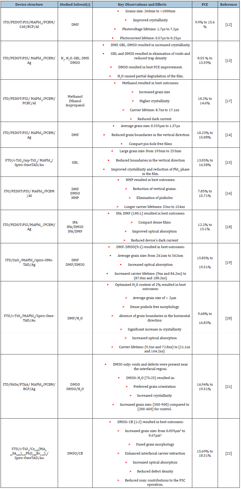
Recently, we investigated use of the mixed solvent-antisolvent in SVA treatment of perovskite films. It was found that by using a DMSO and Chlorobenzene (CB) mixture with an optimized ratio of DMSO:CB (1:2), an increase in the average perovskite film grain size (area) from 0.059μm2 to 0.67μm2 was achieved, along with fused grain morphology, enhanced carrier transfer to the transport layer, increased film optical absorption and reduced trap density. Furthermore, a reduction in the contribution of the mobile ionic density in the perovskite layer to the device operation was observed upon the inclusion of CB in the SVA treatment, along with an increased in the stabilized PCE from 15.69% up to 18.51% [22]. This work further demonstrates the utility of a mixed solvent approach in SVA post-treatments of perovskite films. A summary of the studies covered in this mini review, including the used solvents and their effects on the perovskite films and device performance is shown in Table 1.
Table 1: A summary highlighting the device structures, used single or mixed solvent, key observations and PCE improvement resulting from the SVA treatments applied in the works covered in this mini-review.

Conclusion
In conclusion, this mini review has summarized the recent approaches in the SVA post-treatment on perovskite films, with the aim of improving the performance and stability of the PSCs. In particular, the various single solutions and solution mixtures used in the process as well as their key effects on the perovskite film’s characteristics were reviewed. Overall, SVA post-treatment is a very successfully approach to control various morphological features of perovskite films, including increasing their grain size, eliminating pinholes and voids in the film and eliminating the grain boundaries along the vertical direction of the film, which could facilitate faster carrier transport. Besides, SVA post-treatment has also been shown in multiple works to improve the crystallinity of the perovskite film and reduce the trap density. Another notable observation is the increase in the optical absorption of the films, which can increase the PSCs’ photocurrent. Finally, given the aforementioned positive effects of SVA post-treatment on the perovskite film’s quality, the implementation of interfacial engineering approaches alongside SVA can be a fruitful direction of future research in PSCs to harness the synergistic effects of both SVA treatments and interfacial engineering on improving the performance and stability of PSCs.
References
- Jeon NJ, Noh JH, Kim YC, Yang WS, Ryu S, et al. (2014) Solvent engineering for high-performance inorganic–organic hybrid perovskite solar cells. Nat Mater 13(9): 897-903.
- Rong Y, Tang Z, Zhao Y, Zhong X, Venkatesan S, et al. (2015) Solvent engineering towards controlled grain growth in perovskite planar heterojunction solar cells. Nanoscale 7: 10595-10599.
- Xiao M, Huang F, Huang W, Dkhissi Y, Zhu Y, et al. (2014) A fast deposition-crystallization procedure for highly efficient lead iodide perovskite thin-film solar cells. Angew Chem Int Ed 53(37): 9898-9903.
- Alturisa Mhd I, Wira J, Mardiyati, Herman, Hidayat R (2017) Influences of precursor solution concentration and temperature on CH3NH3PbI3 perovskite layer morphology and the unconverted PbI2 proportion to their perovskite solar cell characteristics. J Phys: Conf Ser 877: 012046.
- Shargaieva O, Näsström H, Li J, Többens DM, Unger EL (2021) Temperature-dependent crystallization mechanisms of methylammonium lead iodide perovskite from different solvents. Front Energy Res 9: 749604.
- Kim SG, Kim JH, Ramming P, Zhong Y, Schötz K, et al. (2021) How antisolvent miscibility affects perovskite film wrinkling and photovoltaic properties. Nat Commun 12(1): 1554.
- An Q, Vieler L, Goetz KP, Telschow O, Hofstetter YJ, et al. (2021) Effect of antisolvent application rate on film formation and photovoltaic performance of methylammonium‐free perovskite solar cells. Adv Energy Sustain Res 2(11): 2100061.
- Tian L, Zhang W, Huang Y, Wen F, Yu H, et al. (2020) Effects of annealing time on triple cation perovskite films and their solar cells. ACS Appl Mater Interfaces 12(26): 29344-29356.
- Dualeh A, Tétreault N, Moehl T, Gao P, Nazeeruddin MK, et al. (2014) Effect of annealing temperature on film morphology of organic-inorganic hybrid pervoskite solid-state solar cells. Adv Funct Mater 24(21): 3250-3258.
- Cao X, Zhi L, Li Y, Fang F, Cui X, et al. (2018) Fabrication of perovskite films with large columnar grains via solvent-mediated ostwald ripening for efficient inverted perovskite solar cells. ACS Appl Energy Mater 1(2): 868-875.
- Zhong Y, Seeberger D, Herzig EM, Köhler A, Panzer F, et al. (2021) The impact of solvent vapor on the film morphology and crystallization kinetics of lead halide perovskites during annealing. ACS Appl Mater Interfaces 13(38): 45365-45374.
- Xiao Z, Dong Q, Bi C, Shao Y, Yuan Y, et al. (2014) Solvent annealing of perovskite-induced crystal growth for photovoltaic-device efficiency enhancement. Adv Mater 26(37): 6503-6509.
- Liu J, Gao C, He X, Ye Q, Ouyang L, et al. (2015) Improved crystallization of perovskite films by optimized solvent annealing for high efficiency solar cell. ACS Appl Mater Interfaces 7(43): 24008-24015.
- Peng H, Lan C, Chen S, Fan P, Liang G, et al. (2019) N,N dimethylformamide vapor effect on microstructural and optical properties of CH3NH3PbI3 film during solvent annealing. Surface and Coatings Technology 359: 162-168.
- Luo J, Qiu RZ, Yang ZS, Wang YX, Zhang QF (2018) Mechanism and effect of γ-butyrolactone solvent vapor post-annealing on the performance of a mesoporous perovskite solar cell. RSC Adv 8: 724-731.
- Kim GH, Jeong J, Yoon YJ, Jang H, Kim S, et al. (2019) The optimization of intermediate semi–bonding structure using solvent vapor annealing for high performance p-i-n structure perovskite solar cells. Organic Electronics 65: 300-304.
- Liu C, Wang K, Yi C, Shi X, Smith AW, et al. (2016) Efficient perovskite hybrid photovoltaics via alcohol-vapor annealing treatment. Adv Funct Mater 26(1): 101-110.
- Sun X, Zhang C, Chang J, Yang H, Xi H, et al. (2016) Mixed-solvent-vapor annealing of perovskite for photovoltaic device efficiency enhancement. Nano Energy 28: 417-425.
- Tian L, Zhang W, Yu H, Peng C, Mao H, et al. (2019) Post-treatment of perovskite films toward efficient solar cells via mixed solvent annealing. ACS Appl Energy Mater 2(7): 4954-4963.
- Ge QQ, Ding J, Liu J, Ma JY, Chen YX, et al. (2016) Promoting crystalline grain growth and healing pinholes by water vapor modulated post-annealing for enhancing the efficiency of planar perovskite solar cells. J Mater Chem A 4: 13458-13467.
- Yi A, Chae S, Lee H, Kim HJ (2019) The synergistic effect of cooperating solvent vapor annealing for high-efficiency planar inverted perovskite solar cells. J Mater Chem A 7: 27267-27277.
- Omer MI, Xizu W, Xiaohong T (2022) Enhancement of the performance of planar perovskite solar cells by active-layer surface/interface modification with optimal mixed solvent-antisolvent post-treatment. Organic Electronics 100: 106349.
© 2022 Tang Xiaohong. This is an open access article distributed under the terms of the Creative Commons Attribution License , which permits unrestricted use, distribution, and build upon your work non-commercially.
 a Creative Commons Attribution 4.0 International License. Based on a work at www.crimsonpublishers.com.
Best viewed in


.jpg)


 Editorial Board Registrations
 Submit your Article
 Refer a Friend
 Advertise With Us
.jpg)


.jpg)


.bmp)
.jpg)
.png)
.jpg)


.jpg)


.png)

.png)


.png)


