- Submissions

Full Text
Polymer Science: Peer Review Journal
Design of the GaN HEMT in Half-Bridge Power Converter
Liu VT*, Liu HR, Hsieh RS and Yan KC
Department of Electrical Engineering, National Formosa University, Taiwan
*Corresponding author:Van Tsai Liu, Department of Electrical Engineering, National Formosa University, Taiwan
Submission: February 12, 2021;Published: March 09, 2021

ISSN: 2770-6613 Volume1 Issue5
Abstract
The introduction of new Wide Band Gap (WBG) power semiconductor devices enables the power converter to break through the limitation of efficiency and power density, so as achieving the goal of high efficiency, light-weight and small size. This article proposes a 200VDC/48VDC 500W output half-bridge power converter, and it uses Gallium Nitride (GaN) High Electron Mobility Transistor (HEMT) to test the efficiency. The frequency of switching can be high up to 250kHz. Mutual verification of the miller effect and the value of probe loading error caused by high frequency.
Keywords: Gallium Nitride(GaN); Half-bridge converter; Miller effect; Probe loading; High Electron Mobility Transistor(HEMT)
Abbreviations:GaN: Gallium Nitride; HEMT: High Electron Mobility Transistor; EMI: Electro Magnetic Interference; SMP: Switching Power Supply
Introduction
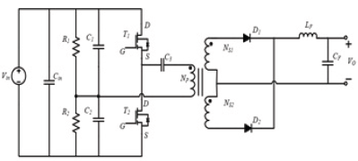
In the era of energy shortage, effective use of energy has always been the main research goal. Switching Power Supply (SMPS) conversion technology has been widely used in daily products. In recent years, switching power supplies are moving towards high efficiency, light weight and small size [1]. In recent years, system designers and product manufacturers have adopted a light-weight, thin, short, and small size as their product features. However, due to materials, Si-MOSFETs have their physical limitations at high frequencies. As a result, because of the limitation of switching frequency and conduction loss, the product design of other components, cores and heat sinks are also limited. After the advent of Gallium Nitride (GaN), changes in materials and advances in manufacturing technology, the switching frequency of Gallium Nitride FETs surpassed the limits of Si-MOSFETs, even high up to 1MHz [2]. Compared with Si-MOSFETs, Gallium Nitride FETs have lower RDS (ON) and conduction losses. However, with the frequency increases, the Miller effect and the RC effect are intensified. The Miller effect generates VGS through CGD and CGS which may affect the operation of the actual circuit. Due to the input capacitance and input resistance measurement of different instruments, the RC effect will cause different waveform results. This kind of converter is applied to higher input voltage. The power switches T1 and T2 and capacitors C1 and C2 can be selected with lower withstand voltage. In addition, the function of capacitors C1 and C2 is voltage division [3], and the two capacitors must be connected in series and have a large capacitance value, that can make capacitor voltage be VI/2. The voltage divider resistors R1 and R2 mainly balance the voltage divider capacitance values C1 and C2 to avoid voltage unevenness caused by electrolytic capacitor error value, that cause the ripple voltage on the secondary side to be larger. The C3 capacitor is mainly used to avoid uneven voltage division, resulting in unbalanced magnetic flux of the transformer and saturation (DC blocking).
Figure 1: System architecture diagram.
Experimental Results
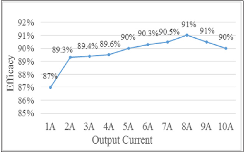
Design an isolated half-bridge circuit in continuous current mode and verify its waveform and efficiency according to the specifications of the physical circuit. Since the dead time is the smallest at 100% load rate, the energy of the leakage inductance has the least impact on the components on the circuit. Thus, the GaN switching voltage is VDS2, the voltage on the primary side of the transformer. The oscillations of VNP, current iNP, and output rectifier diode iD are all minimal. The output voltage VO=47.8V, the output current IO=10A, and the output power is 480W. See (Figure 3), the efficiency of applying GaN to a half-bridge converter at a switching frequency of 250kHz is about 90%. Compared with the traditional half-bridge circuit, the efficiency is 5% higher. And under the same withstand voltage conditions, the RDS (on) of a GaN switch is 5-8 times smaller than the Si switch, and the current is higher. These differences give GaN switches the advantages of high efficiency and high power density. When the driving signal VGS is a low voltage signal, the drain-source (Drain-Source) is turned off and the VDS voltage rises rapidly. It has a higher dv/dt under high-frequency switching, thereby enhancing the Miller effect [4]. As a result, the Miller voltage generated on VGS causes drain-source misconduct and the circuit is destroyed. The VGS(th) of most GaN is only 1.1-1.3V. In the design, attention should be paid to the selection of the driver, the size of the driving resistance RG, the parasitic capacitance of GaN, and the circuit layout to reduce the loop. There are two paths for the Miller effect: red flows to the driver and green flows through CGD and CGS. The current flows to the red reduce the voltage generated by the blue loop and the influence of the Miller effect. The design goal is to make the Miller voltage lower than VGS(th), so that the GaN switch does not conduct.
Figure 2: Design of half-bridge converter with GaN HEMT at 250kHz.
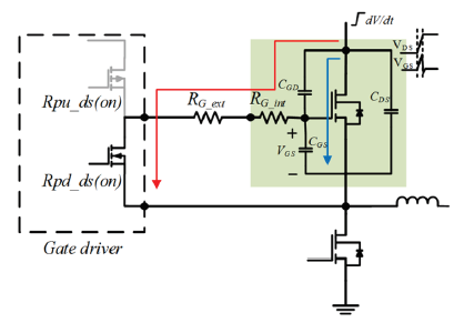
Figure 3: Experimental waveforms of GaN HEMT high-frequency half-bridge converter design. (a) VNP and iNP of main switch S2. (b) iD1, iD2 of diode D1 and diode T2.
Conclusion
The GaN power components have successfully applied to isolate half-bridge converters. The switching frequency of 250kHz is 3-5 times higher than the general switching frequency. That is, the required values of capacitors, inductors, and transformer cores are less than 3-5 times. That is greatly reduce the size of peripheral components and core. As the switch conduction loss decreases, the goal of high power density, high efficiency, and small size have achieved. Although the power density and efficiency of the converter are improved, the shortcomings are relatively amplified. The dv/dt during high-frequency switching is more serious, which makes the Miller effect and Electromagnetic Interference (EMI) problems aggravated. These will be the problems that high-frequency power converters in the future.
Acknowledgement
This research was sponsored by Ministry of Science and Technology of Taiwan under the Grant MOST 109-2622- E-150-019.
References
- Wang K, Wang L, Yang X, Zeng X, Chen W, et al. (2017) A multiloop method for minimization of parasitic inductance in GaN-based high-frequency DC-DC Converter. IEEE Transactions on Power Electronics 32(6): 4728-4740.
- Groot HD, Janssen E, Pagano R, Schetters K (2007) Design of a 1-MHz LLC resonant converter based on a DSP-driven SOI half-bridge power MOS module. IEEE Transactions on Power Electronics 22(6): 2307-2320.
- Boehmer J, Schumann J, Eckel H (2012) Effect of the miller-capacitance during switching transients of IGBT and MOSFET. 15th International Power Electronics and Motion Control Conference (EPE/PEMC), Novi Sad, Serbia.
- Huang Z, Recht F, Wu YJTI, Goleta CA (2014) Printed circuit board layout and probing for GaN power switches. USA.
© 2021 Liu VT. This is an open access article distributed under the terms of the Creative Commons Attribution License , which permits unrestricted use, distribution, and build upon your work non-commercially.
 a Creative Commons Attribution 4.0 International License. Based on a work at www.crimsonpublishers.com.
Best viewed in


.jpg)


 Editorial Board Registrations
 Submit your Article
 Refer a Friend
 Advertise With Us
.jpg)


.jpg)


.bmp)
.jpg)
.png)
.jpg)



.jpg)


.png)

.png)


.png)


