
- About Us
- Information
-

The Author ensures that the research has been conducted responsibly and ethically with adherence to all relevant regulations. read more..
- For Authors
- For Reviewer
- Manuscript Guidelines
- Membership
- Publication Ethics
-
- Journals
- Reprints
- e-Books
- Videos
- Policies
- Contact Us
 COVID-19
- Submissions


Full Text
Novel Research in Sciences
Doping Concentration Profiling of Semiconductors Via Terahertz Deep-Level Spectroscopy, Volume Imaging, and Reflectance Modeling
Anis Rahman*
Applied Research & Photonics, USA
*Corresponding author: Anis Rahman, Applied Research & Photonics, Harrisburg,USA
Submission: December 01, 2022;Published: December 14, 2022
.jpg)
Volume12 Issue 5December , 2022
Abstract
We describe techniques for characterization of doping concentration profile of semiconductors via terahertz deep-level spectroscopy, direct volume-imaging, and an empirical modeling approach. Since the semiconductors are doped mainly via diffusion and ion implantation techniques, the doping concentration is not always uniform across the thickness. Hence, it is important to determine the doping concentration profile across the depth. The deep-level spectroscopy allows (i) to construct a profile of doping concentration across the depth of a wafer or other substrates and (ii) spectral analysis of subsurface layers via absorbance peaks. The direct volume-imaging is used for quantitative dimensional metrology of layers with different compositions such as epitaxial layer thickness and lattice parameter of constituent layers. High resolution images may also be used for lattice scale interface analysis. Finally, an empirical approach has been described for modeling the doping concentration. This empirical route may be used for modeling any dopant-substrate combination. Such model for a given substrate is useful for instantaneous evaluation of doping concentration by the measured reflected intensity of incident T-ray beam. Specific practical examples have been used to described each of the three techniques; all provided via a single experimental setup.
Keywords: Doping concentration, Depth profile, Deep-level spectroscopy, reflectance modeling, volume imaging
Abbreviations: GDMS: Discharge Mass Spectrometry; ICP-MS: Inductively Coupled Plasma Mass Spectrometry; SIMS: Secondary Ion Mass Spectrometry; TNS3DI: Terahertz Nanoscanning Spectrometer and 3D Imager; BLR: Beer-Lambert Reflection; Ge: Germanium; Si: SiliconIntroduction
Semiconductors are routinely doped with foreign atoms for creating carrier concentration that makes them either n-type or p-type. The controlled amount and type of impurities, or dopants, in a semiconductor determine its electronic properties. This fundamental process of incorporating impurities into the crystal lattice is as old as the history of semiconductor industry itself. Several methods have been used in the industry for the measurement of the carrier concentration of doped semiconductors. These include the doping profiling by inverse device methods [1], Seebeck effect [2], the Hall effect [3], Eddy current, Glow Discharge Mass Spectrometry (GDMS), Inductively Coupled Plasma Mass Spectrometry (ICP-MS), and Secondary Ion Mass Spectrometry (SIMS) [4]. Ref. [4] gives a comparison and limitations of the techniques with respect to the Hall effect. The GDMS has a high uncertainty, the ICP-MS has a low resolution and requires a very clean environment, the SIMS need a reference sample, and the Hall effect has an upper limit of detectability of concentration of ~ 1018cm−3 . Also, all of these techniques have an uncertainty between 10% to 20%.
More important, the above-mentioned techniques provide a single value for the total concentration of a specimen. Semiconductors are doped mainly via diffusion and ion implantation techniques [5]. Consequently, the doping concentration is not always uniform across the depth. Hence, it is important to be able to determine the doping concentration profile across the depth. Especially, for the ever-shrinking transistor definition, narrow channels, and waveguide structures, the width of the region of interest is strictly specified; thus, the results exploiting macroscopic techniques such as an electrical contact, etc., are not able to produce a concentration profile across the depth. Moreover, electrical, or optical probes are not able to penetrate deeper; consequently, unable to generate a depth profile of semiconductor wafers.
To this end, a new instrument, a Terahertz Nanoscanning Spectrometer and 3D Imager (TNS3DI) from Applied Research & Photonics (Harrisburg, PA) exploits the Terahertz Radiation (T-ray) for penetrating a semiconductor wafer below the surface. Therefore, it is able to probe both the surface and the sub-surfaces. Since the semiconducting materials are transparent to the T-ray, it can be sequentially focused from the surface to the deeper layers as needed. The TNS3DI also provides three different routes for the concentration measurements. These are (1) deep-level terahertz spectroscopy, (2) direct volume-imaging for measuring the layer thickness and lattice parameter, and (3) using an empirical model for instantaneous quantification of the concentration. In all cases, however, a T-ray beam is vertically focused on the sample, and the measured reflected intensity (Figure 1) is utilized for subsequent computations. Each of these techniques are briefly described in the following sections. In what follows, we first review the principle of carrier concentration dependence of reflection. Then, discuss the measured results via the aforementioned three techniques, after which a conclusion section is added. For the present experiments, two different setups were used: a TN3DI as shown in (Figure 1a) and a TNS3DI as describe above (not shown here).
Figure 1:A laboratory setup for semiconductor wafer measurements. (a) A wafer sample is mounted on the nanoscanner in the vertical mode, suitable for small samples. (b) A wafer may be mounted in the horizontal mode for large wafers. Reflectance measurement can be done in both vertical and horizontal configurations.

Review of Theoretical Approach
Approaches by which the resistivity may be computed from optical measurements is given in refs. [6, 7] for the specific cases of polycrystalline metallic film, and for bulk silicon, respectively. While terahertz (T-ray) is not quite an optical approach, herein we discuss the principle of impedance dependence of reflectance of T-rays. Since the reflectance is a function of the impedance for any substrate, measurement of reflectance allows resistivity and related calculations such as the carrier concentration. In the linear regime, the dielectric function ∈ and the susceptibility χ are defined in terms of the free-space electric field E, the displacement field D, and the polarization field inside the semiconductor, P, by the following relations [8]
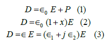
where, ∈0 is the permittivity of free space; and ∈and χ are dimensionless quantities, each of which can completely describe the optical properties of semiconductors. The refractive index of the material is related to ϵ and given by
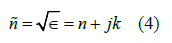
The real and imaginary parts of the refractive index, and k, which are also referred to as the optical constants, embody the linear optical property of the material. The imaginary component, k, denotes absorption of optical energy by the semiconductor. In the spectral regions where, absorptive processes are weak or absent, k is very small, whereas in regions of strong absorption, the magnitude of k is large. The reflection from a surface is given by:
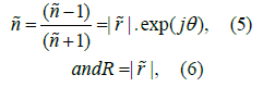
where, r is the complex reflection coefficient and R is the power reflectance. The transmission T is then calculated from T = (1− R) . [6] the authors showed that when the reflectance R, is influenced by the grain boundary effect, R is expressed by,
where, Z is the surface impedance, and c is the speed of light. The authors’ solution for Z, obtained by solving the Maxwell’s equations, depends on many parameters including the bulk conductivity, and a scattering parameter, (γ ) . The authors have also shown that the reflectance of Ag films is a linear function of the scattering parameter (γ ) with minor wavelength (λ ) dependent dispersion up to(λ ) =10μm. While T-ray wavelengths span up to millimeters, a calibration could be conducted to fit in an empirical model, as discussed below. The formulations shown in Eq (7), however, is suitable for very specific cases as described in their paper [6]. In the present work, we demonstrate exploring the terahertz regime for measurement of doping concentration and other physical parameters by measuring the T-ray reflectance. An example of computing the boron concentration of a doped wafer is described. The T-ray deep-level spectroscopy and empirical models are also described below.
Experimental
A new instrument from Applied Research & Photonics (ARP) (Harrisburg, PA), the terahertz nanoscanning spectrometer and 3D imager (TNS3DI), has been designed such that it offers the capabilities for the aforementioned measurements for the semiconductors. The TNS3DI has been used for the present investigations. (Figure 1) exhibits mounting of samples (wafers) with two different orientations. Either orientation may be used for the required tasks. For the present work, all samples were mounted one at a time, in the vertical orientation. Measurements were carried out with the front-end software of the TNS3DI. For the volume image generation, each sample was scanned over a user-selected three-dimensional space. That is, first a line-scan was conducted on the X-axis on the X-Y plane; then the line-scan was repeated to cover the whole X-Y plane for a single surface. The T-ray was then focused on a plane below the surface by programmatically adjusting the Z-stage by a user-defined increment of depth. The surface scan was then repeated for covering the entire volume. The resulting intensity matrix, termed as the Beer-Lambert Reflection (“BLR”) matrix is subsequently used for the volume image generation via an algorithm described elsewhere [9].
Results and Discussion
Deep-level spectroscopy
Figure 2:(a) Evolution of the terahertz interferogram (deep-level T-ray signal) across the depth (t) of sample D02, Ge over Si. (b) deep-level terahertz interferogram across the depth (t) of an epitaxial semiconductor, SiGe over Ge (reproduced from [9]). (*) represents the scaleddown values of the reflected intensity of T-ray (counts).

The reflection dependence of doping concentration gives the total concentration of a sample. A concentration profile across a given depth, however, is often of interest. Terahertz reflectance spectroscopy is uniquely deployed for this task. Since T-ray penetrates most materials including the semiconductors, a reflected time-domain signal of a focused terahertz beam is acquired as a function of depth; thus, probing the depth dependence of the concentration. The results of T-ray deep-level spectroscopy are described below. Here an epitaxial semiconductor’s deep-level terahertz spectral evolution is shown in (Figure 2). (Figure 2a) exhibits the evolution of the terahertz interferogram (deep-level T-ray signal) across the depth of a sample D02, which is composed of a deposited layer of Germanium (Ge) over Silicon (Si), and (Figure 2b) exhibits the same for a sample D10, which is composed of a layer of Silicon-Germanium (SiGe) over the Ge layer of sample D02 [10] (both reproduced from ref. [9]).
Figure 3:(a) Slightly tilted view of the deep-level T-ray signal across the depth (t) of the sample D10 (SiGe over Ge). (b) The peak value of the deep-level T-ray signals vs. depth. Layered pattern visible from peak values.

Figure 4:(a) Evolution of the terahertz interferogram (deep-level T-ray signal) across the depth of an undoped LiNbO3 substrate and (b) deep-level terahertz interferogram across the depth of a doped LiNbO3 waveguide.

Figure 5:The peak value (reflected intensity) of the signals as a function of depth. The peak values may be calibrated for computing the carrier concentration profile along the depth.

The spectral analysis of these deep-level T-ray signals are discussed in ref. [9]. (Figure 3a) shows a slightly tilted view of the same signals in (Figure 2b), and (Figure 3b) exhibits a plot of the peak values of the signals in (Figure 2a). The wavy nature of the peak value is assumed to be indicative of layered pattern of the sample, as indicated in (Figure 3b). The peak values may be calibrated for computing the carrier concentration profile along the depth with respect to the depth profile of a blank (undoped) reference substrate; for which, an experiment is to be designed to determine the depth profile of doping concentration of different wafers with varied degree of doping. Once determined, these profiles will serve as a library for subsequent measurement of doping concentration profile via T-ray deep-level spectroscopy. However, an example of the concept is demonstrated in (Figure 4) Here a LiNbO3 sample was used. The deep-level terahertz interferogram was measured for both undoped substrate and doped sample of LiNbO3 [11] up to the depth of 14μm at an interval of 1μm. (Figure 4) exhibits the interferograms vs. depth over 14μm. (Figure 5) exhibits the peak values (left Y-axis) of the interferograms for both undoped (red line) and doped LiNbO3 samples (blue). The right Y-axis of (Figure 5) exhibits the computed difference of the interferogram peak values (green), which gives the depth profile of doping concentration in terms of the reflected intensity,

Direct volume imaging
Figure 6:Volume image (1μm)3, of an epitaxial semiconductor is used to measure thickness of different layers. adapted from ref [9].

Volume imaging via T-ray route allows to inspect the lattice profile from the surface into a specified depth. Thus, it aids in a visual inspection and metrology via graphical analysis of the lattice structure. Since the doped lattice has a slightly different lattice constant compared to the undoped region, a quantitative measurement and profiling is possible as described below. Here, the advent available from the TNS3DI was utilized for imaging a small volume of the present samples for the inspection of lattice structure across the thickness on a layer-by-layer basis. (Figure 6) exhibits an example of a volume (3D) image of an epitaxial semiconductor (sample courtesy of IMEC, Leuven, Belgium [10]), see ref [9] for details. Different layer thicknesses were quantified via graphical analysis, as reported in [9]. Another example is from the perturbation of nickel lattice by alumina nanoparticle [12]. (Figure 7) exhibits a volume image of a metallic nickel film where lattice deformation due to alumina nanoparticle inclusion is visible. The graphical analysis along the cursor of (Figure 7) is displayed in (Figure 8). The lattice plane separation may be computed from (Figure 8) by the standard technique of full width at half maximum (FWHM) analysis which then could be related to the doping concentration via calibration. That is, lattice spacings of samples with known concentration will be used for arriving at an empirical formula for computing the concentration profile of unknown samples from measured lattice spacing of a given specimen.
Figure 7:Three-D Lattice image (1μm)3, of nickel impregnated with alumina nanoparticle via plasma spray-deposition [12]. The lattice planes are deformed due to the inclusion of alumina nanoparticle. This may be used for lattice constant measurement and for inspecting lattice perturbation across the depth. Graphical analysis along the cursor (see arrow) is shown in (Figure 8).

Figure 8:Graphical analysis of the lattice plane perturbation along the cursor in (Figure 5). Here, the lattice plane dilation due to the inclusion of alumina nanoparticle can be quantified.

Modeling for concentration measurement
For this option, a set of samples with varying known doping concentration was used to construct an empirical model from the measured T-ray reflectance. Once the modeling is done, the T-ray reflectance from the TNS3DI allows instantaneous measurement of carrier concentration of unknown samples, either for laboratory measurement or for industrial quality control. An example of concentration vs. reflectance modeling of boron doped silicon wafer is shown in (Figure 9). In this case, the samples were mounted on the TNS3DI one at a time and the reflectance was recorded for 60 seconds for each sample. The average of reflectance data over 60 seconds was used for modeling. The model (the solid line) shown in (Figure 9), is given by the Lorentzian cumulative eqn.
Figure 9:Measured T-ray reflected intensity vs. concentration model (line) fit with data (circles). This model may be used for instantaneous computation of doping concentration.

where, conc N is the doping concentration, R is the measured reflectance in counts, and a, b, c are the fit parameters having the values, a = 1.26799 ×10⁶ ± 6.90456 ×10¹⁴ , b = 2.44814 ×10⁸ ±1.56199 ×10⁶ and c = −5.1332×10⁶ ± 756460.0314. (Figure 9) exhibits data (dark dots) of epitaxial wafers with different doping concentrations and thickness on Si-substrate [13]. The resistivity of these samples was measured by 4-point probe method and the thickness were measured by an ellipsometer, from which the concentration was calculated [13].
Conclusion
This paper describeds techniques for measuring the doping concentration of semiconductors. A new cameraless imaging technique combined with deep-level spectroscopy enables measurements of the doping concentration profile across the thickness of a doped wafer. In addition, an empirical modeling was developed from known concentration data of boron doped silicon samples with a range of doping concentrations. The new technique of TNS3DI offers advent for concentration depth profiling by deeplevel T-ray spectroscopy where the depth dependent evolution of the T-ray interferograms are measured. The peak values of the depth dependent interferograms of a doped sample are compared to the same of an undoped substrate; the difference between the two generates the depth profile. The technique can be used for both routine laboratory investigations and inline monitoring of the doping process for semiconductors. To our knowledge, this is the first instrument of its kind offering plurality of analyses for doping concentrations’ quantitative analysis, and process development related testing.
Acknowledgment
The authors wish to express thanks and gratitude to Mr. Chung Tae Kim, PhD/CTO, of Mindseye Co., Ltd. 5F 503, 65, Dongpyeon-ro 13 bean-gil, Dongan-gu, Anyang-si, Gyeonggi-do, South Korea, for sending the samples with measured data.
References
- Avner Friedman (1995) Doping profiling by inverse device methods. Mathematics in Industrial Problems Part 7, Springer-Verlag, USA, pp. 130-146.
- Pó JM, Brito MC, Maia AJ, Silva JA, Serra JM, et al. (2013) Measurement of the dopant concentration in a semiconductor using the seebeck effect. Meas Sci Technol 24(5): 6.
- Schroder DK, Braggins TT, Hobgood HM (1978) The doping concentrations of indium-doped silicon measured by Hall, C -V, and junction-breakdown techniques. Journal of Applied Physics 49(10): 5256-5259.
- Aurélie F, Benoit M, Jordi V, Sébastien D, Anne K-C, et al. (2016) Comparison of characterization techniques for measurements of doping concentrations in compensated n-type silicon. Energy Procedia 92: 691-696.
- Peter VZ (2000) Microchip fabrication: A practical guide to semiconductor processing. (4th), McGraw Hill, USA.
- Dimmich R, Warkusz F (1982) Optical reflectance and electrical resistance of polycrystalline thin metallic films. Phys Stat Sol 72(1): 117-122.
- Degallaix J, Flaminio R, Forest D, Granata M, Michel C, et al. (2013) Bulk optical absorption of high resistivity silicon at 1550nm. Optics Letters 38(12): 2047-2049.
- Gerald Burns (1985) Solid state physics. Surface Science, Academic Press Inc, USA.
- Rahman A, Rahman AK, Yamamoto T, Kitagawa H (2016) Terahertz Sub-Nanometer Sub-Surface Imaging of 2D Materials. J Biosens Bioelectron 7: 1-8.
- The D02 and D10 samples are courtesy of IMEC, Leuven, Belgium.
- The lithium niobate samples were provided courtesy of SRICO manufactures, USA.
- Anis R, Francis T, Aunik KR, Carl P, Robert G (2019) Lattice dilation of plasma sprayed nickel film quantified by high resolution terahertz imaging. Nov Res Sci 2(4): 1-9.
- Chung Tae Kim, Samples and data are courtesy, Korea.
- Rahman A, Rahman AK (2016) Terahertz spectroscopic analysis and multispectral imaging of epitaxially grown semiconductors with nanometer resolution. J Biosens Bioelectron 7: 4.
© 2022 Anis Rahman. This is an open access article distributed under the terms of the Creative Commons Attribution License , which permits unrestricted use, distribution, and build upon your work non-commercially.
Editor In Chief


.jpg)


Signup for Newsletter

Quick Links
 Editorial Board Registrations
 Submit your Article
 Refer a Friend
 Advertise With Us
Our Recent Edition

.jpg)


Top Editors


.jpg)


.bmp)
.jpg)
.png)
.jpg)


.jpg)


.png)

.png)


.png)


Financial Support

Sponsors

Latest e-Books

Latest Video

 a Creative Commons Attribution 4.0 International License. Based on a work at www.crimsonpublishers.com.
Best viewed in
a Creative Commons Attribution 4.0 International License. Based on a work at www.crimsonpublishers.com.
Best viewed in