
- About Us
- Information
-

The Author ensures that the research has been conducted responsibly and ethically with adherence to all relevant regulations. read more..
- For Authors
- For Reviewer
- Manuscript Guidelines
- Membership
- Publication Ethics
-
- Journals
- Reprints
- e-Books
- Videos
- Policies
- Contact Us
 COVID-19
- Submissions


Full Text
Novel Research in Sciences
Silicon Technology as the Core for Semiconductor, Solar Cell and Optical Fiber Initiatives in Bangladesh: An Economic Model and Projection
Anis Rahman*, Md Mahadee Hassan and M Shahidul Islam
Applied Research & Photonics, USA
*Corresponding author: Anis Rahman, Applied Research & Photonics, USA
Submission: June 03, 2022;Published: June 15, 2022
.jpg)
Volume11 Issue2june, 2022
Abstract
This paper outlines the basic technology and economic model of the core silicon technology. Silicon is the second most abundant element on the earth’s crust but there is no specific deposit or mine for silicon. The only source for silicon is “sand” that the earth has an abundant supply. Here we outline the basic steps of manufacturing silicon ingot and wafers. It is projected that, once produced, these products will gain immediate market access, thus creating economic activities in a reasonably short period of time. The three initial products that could stem from the basic silicon ingot are silicon wafers, for both semiconductor and solar cell applications, and optical fiber for communication. This report focuses on the essential silicon technology to produce silicon ingot, and silicon wafer, as the first step. Finally, the historic data available for the silicon wafer consumption per year have been modeled with the well-known Bass diffusion model. It was found that with modified parameters, the Bass model fits the historic data well and the same model allows a projection for a few years in the future. This projected economic activities, therefore, encourages a social transformation towards a technological self-sufficiency.
Keywords: Keywords: Silicon technology; Bass diffusion model; Silicon wafer consumption; Social transformation; Technological self-sufficiency
Introduction
Silicon processing technology is at the root of three important technologies that are indispensable for the modern society. These are (1) semiconductor wafers for Integrated Circuit (IC) fabrication, (2) silicon wafers for solar cell fabrication and (3) silicon dioxide (glass) for optical fiber fabrication. Thus, once the core technology of silicon processing is established, all three of the above crucial technologies become easily achievable and producible. The economics of each of these technologies, and derived products, are well known. The worldwide consumption of these three areas is in a few $100s of billions each. Therefore, if one can tap into any or all three of these technologies, that is expected to produce significant economic activities. The nature of each of these three technologies are such that their demand will only be increasing for indefinite future while saturation may arise in the distant future. This paper outlines the basic technology and economics of the core silicon technology. Silicon is the second most abundant element on the earth’s crust but there is no specific deposit or mine for silicon. The only source for silicon is “sand” that the earth has an abundant supply. Here we outline the basic steps of manufacturing silicon ingot and wafers. It is projected that, once produced, these products will gain immediate market access, thus earning foreign currencies in 3-5 years period. The three initial products are silicon ingot and silicon wafers, for both semiconductor and solar cell applications, and optical fiber for communication. Therefore, we focus on the core silicon technology as the first steps to produce silicon ingot, silicon wafer for ICs. Other products, viz., silicon wafer for solar cell, followed by the optical fiber will be discussed as the next steps. In general, development, prosperity, betterment of human lives and the improvement of the socio-economic conditions are always good things. Like the air we breathe that flows without any boundary, good things flow all over the world regardless of where they originate; be it in Bangladesh or USA. Bangladesh is at the juncture of transitioning from a developing country towards a developed country. This transition requires simultaneous development in multiple sectors, including technology, new products, education, healthcare, water, electricity, and many more. In doing so, Bangladesh’s objective should not only be to solve her own problems, but also make an effective effort to solve a few problems of the entire humanity on the planet earth. As the history suggests, when one identifies a bigger problem that encumbers a bigger (world) population as one’s own problem, the solution (if and when achieved) offers a bigger reward. For example, if Bangladesh is able to take initiatives to alleviate the worldwide shortage of silicon wafer, it will bring a better reward for the whole humanity. Because the world is now facing critical shortage of semiconductor chips, where the geopolitical factors are playing important role, Bangladesh could help alleviate the problem by becoming a supplier of the raw silicon wafers which is the basis for making all chips. Additionally, new applications such as the automotive and electric vehicles, require new kind of ICs for which different wafers are needed. High temperature (under the hood) and high voltage applications ICs are made from Silicon Carbide (SiC). So, one can contemplate production of SiC wafers when the basic production system is operational.
Silicon Wafer Manufacturing
While the world is currently suffering from shortage of silicon wafers, the situation is even more extreme in the automotive industry. The semiconductor shortage, indeed, has been at the center of many economic setback for several industries, and it has hit the automotive industry harder than most others [1]. Thus, need for new sources of silicon production is important.
The silicon wafer: The foundation of IC fabrication
The microscopic circuit patterns of the ICs are built by layers after layers of various materials, and these steps are repeated for a few hundred times before the chip finally becomes a reality. However, it all begins with a silicon wafer [2] as the basis for any chip development and fabrication. Silicon wafers (Figure 1) are created from sand as the starting material. In particular, the sand that is rich in quartz content are more suitable than others. As pointed out before, silicon is the second most abundant element in the earth’s crust, comprising of about 27% and exceeded only by oxygen at 47%. Since metallic silicon does not occur naturally in the pure form, which is needed for ICs and solar cell fabrication, the sand is processed for extracting the silicon. The electronic grade silicon requires the highest purity silicon, that must not contain even one atom of impurity in a billion silicon atoms, a purity of 99.999999999%. The silica sand is often quarried for this purpose that has quartz (silicon dioxide) concentrations of >95%. Nonetheless, all sand requires purification, but lower quartz content sand requires more rigorous purification that starts by heating the sand with a reducing agent, carbon, to produce carbon monoxide and silicon. The product of this process, known as Metallurgical Grade Silicon (MG-Si), produces 99% pure silicon. This MG-Si is used for solar cell wafer fabrication without further purification (Figure 1). But for IC fabrication, ultrapure Electronic Grade Silicon (EG-Si) is required which needs additional processing before making the ingot (aka boule). In addition to being very pure, the silicon used in the ICs must also be made of a perfect single crystal of a designated crystal plane (e.g., <1,0,0>). This perfect single crystal is grown by a common technique such as the Czochralski (chokh-RAL-skee) process or the Floating Zone process.
Figure 1: A stack of wafers (1 2 3 4 5 …) usually remains in a wafer cassette (adapted from stock photo).

Building an ingot (or boule)
The silicon extracted from sand becomes small chunks of silicon. It is then purified, and metallic silicon is formed known as polysilicon (MG-Si). For making the single crystalline ingot, the polysilicon is heated in a suitable crucible until it melts into a highpurity liquid. This liquid silicon is then solidified into a silicon rod, or ingot, via the Czochralski method, a small seed crystal of silicon of a chosen crystal plane is placed in contact with the top surface of the molten silicon in the reservoir. This seed crystal defines the crystal structure of the whole ingot and subsequently, the wafers. The seed crystal is slowly “pulled” up away from the melt, thus, silicon atoms deposit on the bottom surface, perfectly matching and extending the crystalline lattice of the seed. A large cylindrical ingot or boule is produced (Figure 2 & 3). The boule diameter is determined by calculated pulling speed and the rate of rotation and its length is determined by the capacity of the pulling unit. This is how the wafers become round. Up to 3-meter-long silicon boules are produced while 1-meter and 2-meter-long boule are also common. Special semiconductors such SiC producers usually work with shorter length boule such as 500mm. When the boule is ready, it is sliced into wafers less than a millimeter thick. Finally, the wafer surfaces are polished to atomically smooth, and the edges are shaped to remove cracks. Some wafers have an end cut off to create a small flat side; this is called just a flat. Some wafers may have two flats or some others may have a notch instead of a flat. The flat or notch is required for alignment purposes for the subsequent processes of IC fabrication. Before it is completely cooled, the cone-shaped ends of the ingot (Figure 2) are cut off while the body is sliced into thin wafers of uniform thickness with sharp diamond saw (blade). Thus, the ingot’s diameter ultimately determines the size (diameter) of a wafer. In the early days of the semiconductor industry, wafers were only three inches in diameter. Since then, wafers have been growing bigger in diameter. Because larger wafers result in a greater number of chips per wafer, bigger wafers lead to higher productivity. The largest wafer diameter used in semiconductor fabrication today is 12 inches or 300mm, while the 18” (450mm) wafers are on the way. Figure 3 exhibits a sketch of two different views of a machine used for producing the silicon boule. Figure 4 shows an actual boule of 200mm dia and 2.5m long; an author is seen standing next to the boule. Since this ingot is subsequently sliced into thin wafers of ~500μm or less thickness, the boule in Figure 4 will make ~4,500 silicon wafers at 500μm thickness each, accounting for the kerf-loss during slicing. Smaller diameter wafers are thinner. Some wafers are as thin as only 50μm. In this case the yield per meter of the ingot is higher.
Figure 2: (a) Ingot pulling furnace schematic. (b) the conic object (ingot) is cut to a uniform diameter, polished and eventually becomes a wafer.

Figure 3: Anis Rahman standing next to a ~2.5m long silicon ingot when visiting the manufacturer at the Semicon West 2021. A demo machine is seen on the left. The ingot is sliced into thin wafers of ~750 μm thick. This ingot will make ~3,000 silicon wafers. Smaller diameter wafers are thinner. Some wafers are as thin as only 50μm when the yield >10,000 wafers per meter of the ingot (including the kerf-loss).

Figure 4: Two different views of a machine for making the silicon boules.

Economics of Silicon Boule and Wafer
Rising production costs have been a major driver pushing up premiums for the silicon ingot market and related products. The silicon Wafer Market is segmented by the diameter of the wafer (150mm, 200mm, 300mm and 450mm); application segments such as consumer electronics, industrial, computing, and automotive; and by geography.
Market projection
While silicon ingot and/or optical fibers are not new products, however, planning its production at a new setting, especially in a developing country, still requires rigorous business considerations. From this point of view, it is similar to developing and launching a new capital equipment product. When a new product is introduced by any entity, an estimate for its future sales, profits, and other impacts on objectives are important. The appropriate salesforecasting model varies with the type of the new product and situations such as the degree of novelty of the product and the degree of product repurchase ability. Frequency of purchase is low for high-cost products such as a piece of capital equipment for the semiconductor industry.
As such all new products must be adopted by a purchasing population who initially would not know about them. The adoption of new products (e.g., a capital equipment) is a complex process, especially for big manufacturers who are the main users of such complex machineries. The purchasing process depends mainly on the following: (1) The diffusion of innovations: i.e., how the knowledge of a new idea, goods, or services, are assimilated into a social system comprised of knowledge workers such as the scientists, engineers, technicians, researchers, etc. (2) The diffusion process of knowledge, which is the spread of an idea or the market penetration of a new product from its source of creation to its ultimate users or adopters. (3) The new technology adoption process, which involves the steps an individual or an entity goes through from the time s/he/they learn about an innovation until final adoption (the decision to use an innovation regularly). In case of a capital equipment, multiple individuals are involved who represent the institution. In what follows, we consider a case for a well-known technology and product that will be initiated for the first time in a less developed environment. Therefore, a “whatif” scenario is formulated based on target usages in specific or collective areas. However, before going to the details of the model and forecast, it is useful to review the market potential of the proposed products.
Market overview of silicon technology
The semiconductor industry has been a significant driver behind the critical innovations in sectors like Electronics, Automobile, and Automation. Semiconductor technology has established itself as the building block of all modern technologies. The advancements and innovations in this field are immediately impacting all downstream technologies. Semiconductor wafers remain the core component of various microelectronic devices and forms the electronics industry’s cornerstone. With digital economy and electronic mobility denoting the current trends in the technology landscape, these products are finding applications in many devices. Similarly, the solar energy is another important sector that depends on silicon technology while the optical fiber forms the core of digital communication. Before COVID-19, by the end of 2018, buyers at Integrated Device Manufacturers (IDMs) and semiconductor foundries (aka, Fabs) were expecting silicon wafer prices to increase over the next five quarters in 2019 and 2020 because of constrained supply of 6-in., 8-in and 12-in. wafers. There were several reasons for the tight supply and increased prices for silicon wafers, including robust demand for semiconductors, more Chinese fabs coming online, and a lack of investment in capacity by silicon wafer manufacturers. Major wafer manufacturers, such as Global Wafers, Shin-Etsu Handotai, SUMCO and SK Siltron, have not invested a lot in new capacity because, until recently their existing facility was producing enough foreign currency. With the outbreak of the COVID-19 pandemic, the semiconductor demand increased in the second quarter of 2020, owing to the growth in stock clearance of the end products across end-user industries. SEMI, a Silicon Valley based leading semiconductor organization, reported in its annual silicon shipment forecast for the semiconductor industry that global silicon wafer shipments were set to increase by 2.4% Y-o-Y in 2020, with growth continuing in 2021 and shipments reaching a record high in 2022. Figure 5 exhibits the public domain data of shipment of silicon wafers from 2018 onward with a projection until 2023, in the units of millions of square inches. While the unit used in Figure 5, the “square inches,” normalize the volume of the wafers regardless of their size, the numbers in Figure 5 may readily be appreciated by converting to the number of wafers. For instance, an 8” wafer has an area of 50.26sq. inch. Thus, the number of wafers shipped in 2018 becomes 249.495 million. For 12” wafer the area is 113.09sq. inch; thus, the number of wafers equal to 110.887 million. In reality, wafers of different sizes are shipped. Therefore, an exact number of each size of wafers need to be known. These databases are available to purchase from the SEMI. Currently, advances in wireless computing devices, such as tablets and smartphones, have increased design activity among semiconductor designers, resulting in high demand for silicon wafers (Figure 6). Also, favorable government policies across the emerging economies like China, India, and Malaysia, for example, have created enormous opportunities for the semiconductor industry, which is expected to expand the silicon wafer market’s scope in the future. For instance, the policy framework published by the State Council of the People’s Republic of China aims to make advanced semiconductor packaging solutions a technology priority across the semiconductor industry. This also sets a trend for others to develop and harness the opportunity created. Another factor is the size of wafers being manufactured, which has progressed from 75mm (3”) to up to 450mm (18”). At the same time, drastic instance of collaboration and consolidation, caused the number of suppliers decreasing from more than 20 vendors in the 1990s to five prominent players dominating across the different diameters of wafer being produced today. With the increasing demand for semiconductor wafers, the market has been witnessing acquisition activities for extending production capacities and supply chain operations. In November 2020, Taiwan’s GlobalWafers announced that it is in talks to acquire Siltronic, a German manufacturer of silicon wafers, for €3.75 billion, adding to a record year for deals in the global semiconductor industry. A surge in demand for various chips is resulting in shortages for select foundry capacity as well as fab equipment.
Figure 5: Global consumption of silicon wafers is projected to reach ~14 billion in 2023. Source: SEMI.

Figure 6: Projected revenue in billions of dollars showing an increasing trend. While the actual dollar numbers are not available, it is usually in the 100s of billions.

The Diffusion Model Projection of Silicon Technology
The above market review clearly indicates that the demand for the silicon boule and the wafers obtained from the boule always exhibit an increasing trend. Unlike many other sectors where the demand fluctuates, demand for silicon and related products is continuously increasing. So, one can make a realistic projection by applying the Bass diffusion model. The Bass diffusion model was developed by Frank Bass [3] which describes the process of how new products get adopted as an interaction between the current users and the future users. It has been described as one of the most famous empirical generalizations in marketing and management science. A diffusion model, or more precisely diffusion of knowledge model, produces a life-cycle sales curve based on a small number of parameters. The parameters may be estimated by analogy to the historical data of similar new products introduced in the past, and by early sales returns as the new product enters the market. Bass Model is designed to answer the question: “How many customers will eventually adopt the new product and when?” This is indeed a crucial question to answer, especially for the products that are meant for the populous. This is important also because launching a new product requires a lot of investment during the development phase, before any profit can be realized. More important, investors must know in advance that if their investment will result into something good for people. However, in case of a core technology such as the silicon technology-based products of the present work, where there are only a few potential customers worldwide, yet each will require a huge number of the same product (e.g., silicon wafer) as described before. In such situations, the application of Bass diffusion model requires some modifications. The considerations are the followings. (i) There are only a few buyers for these products. (ii) Given that there is a shortage in the market, and the worldwideThe above market review clearly indicates that the demand for the silicon boule and the wafers obtained from the boule always exhibit an increasing trend. Unlike many other sectors where the demand fluctuates, demand for silicon and related products is continuously increasing. So, one can make a realistic projection by applying the Bass diffusion model. The Bass diffusion model was developed by Frank Bass [3] which describes the process of how new products get adopted as an interaction between the current users and the future users. It has been described as one of the most famous empirical generalizations in marketing and management science. A diffusion model, or more precisely diffusion of knowledge model, produces a life-cycle sales curve based on a small number of parameters. The parameters may be estimated by analogy to the historical data of similar new products introduced in the past, and by early sales returns as the new product enters the market. Bass Model is designed to answer the question: “How many customers will eventually adopt the new product and when?” This is indeed a crucial question to answer, especially for the products that are meant for the populous. This is important also because launching a new product requires a lot of investment during the development phase, before any profit can be realized. More important, investors must know in advance that if their investment will result into something good for people. However, in case of a core technology such as the silicon technology-based products of the present work, where there are only a few potential customers worldwide, yet each will require a huge number of the same product (e.g., silicon wafer) as described before. In such situations, the application of Bass diffusion model requires some modifications. The considerations are the followings. (i) There are only a few buyers for these products. (ii) Given that there is a shortage in the market, and the worldwide demand for these products are only going up, therefore, each buyer will need billions of units of the same product (e.g., wafers). Hence, in reality, each buyer represents billions of individuals, as would have been the case for a retail product. As such, the factor m in the Bass model (see below) that represents the maximum potential number of adopters is not a constant, rather a compound function. This is discussed further below. (iii) The original Bass model is a pre-Internet era model. Hence the effect of the Internet must be incorporated. Considering these factors, a modified Bass model is formulated below. It is appropriate that one would be forecasting the first purchase of a new product for which no closely competing alternatives exist in the marketplace. Managers need such forecasts for new technologies or major product innovations before investing significant resources in them. The Bass model offers a good starting point for forecasting the long-term sales pattern of new technologies and new durable products under two types of conditions. (1) The firm has recently introduced the product or technology and has observed its sales for a few time periods; or (2) the firm has not yet introduced the product or technology, but it is similar in some way to existing products or technologies whose sales history is known. For the silicon technology of the present report, the later condition is applicable.
Assumptions of the Bass Diffusion Model
The Bass model of 1969 [3] made the following implicit and
explicit assumptions:
i. An adoption process for a new product is binary; that is a
consumer either adopts or waits.
ii. Maximum number of potential buyers (m) is constant
iii. Eventually, all m will buy the product
iv. No repeat purchase, or replacement purchase
v. The impact of the word-of-mouth is independent of adoption
time
vi. Knowledge diffusion is considered independent of substitutes
The marketing strategies supporting the innovation are not explicitly included as such the basic Bass model leaves out the effects of influence of mass-media communication and the recent Internet factors. Consequently, a modified model is presented below following the description of the basic Bass model. According to this model [3], sales S(t), is the rate of change of installed base (i.e., adoption) f(t), multiplied by the ultimate market potential m:
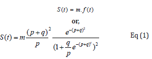
The parameter p is called the coefficient of innovation, external influence, or advertising effect. The parameter q is called the coefficient of imitation, internal influence, or word-of-mouth effect. The average value of p has been found to be 0.02 and is often less than 0.01. The average value of q has been found to be 0.38, with a typical range between 0.3 and 0.5. It is notable that Eq (1) does not consider the Internet effect [4] that is very important in this era of network advantages and social media, etc. Therefore, we propose to add a factor α to Eq (1) that accounts for the Internet factor,
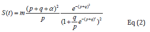
In the modified statement, it is further implied that the market potential m is a parameter determined for each market space (as opposed to being a constant). It is worth noting that the factor m is also time dependent, a deviation from Bass’s original hypothesis. In effect, the ultimate market potential, m is the factor that depends on a population of knowledge worker among which an early adopter may be found. Thus, one assumes via the diffusion theory that the knowledge of a new technology will “diffuse” among this population as a function of time. Eq (2) also consider the factor m as a constant like the original Bass model, but in reality, m will vary based on a given product, target population, and time. The consideration for the silicon technology is the fact that there are only a few hundred semiconductor Fab locations worldwide who the potential buyers of the finished wafers are. The Wikipedia lists the current number of worldwide fab locations is 534 [5]. As depicted in Figure 5, these small number of fabs are consuming billions of wafers each year, and the demand is only going up. The factor m, therefore, must include this fact. As such, it is reasonable to express the market potential as,
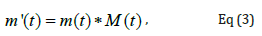
where, M(t) is the number of units to be purchased by a single buyer; that is the number of wafers utilized per semiconductor fab. Thus, it is fortuitous for the case of the silicon wafers that the actual number of wafers shipped is well reported [6] as shown in Figure 5. Obviously, in this case the factor M(t) is >> m(t), hence we rewrite Eq (2) as,
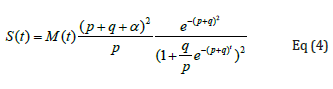
The data from Figure 5 was used as the factor m^’ (t)≈M(t), and was fit by a second order polynomial, as shown in Figure 7. The same polynomial was also used for projection into a few years as shown in Figure 7. Utilizing the foregoing, it is possible to estimate the total number of wafers to be consumed per year, S(t), given by Eq (4). Bass found that his model fit the data for almost all product introductions, despite a wide range of managerial decision variable, e.g., pricing and advertising. This means that decision variable can shift the Bass curve in time and amplitude, but that the shape of the curve is always similar [7]. Total sales dollars are simply a multiplicative factor of the adopters and unit price. However, in view of Figure 8, it is evident that the wafers consumption (in millions of sq. inch, “MSI”) exhibits an increasing trend over time. This is because the S(t) given by Eq (4) is dominated by the trend of M(t) derived from the reported data as shown in Figure 7. Thus, the modified Bass model, as described herein, not only fits the historical data for silicon wafer consumption, but it also predicts an increasing trend of the of the same for a few years in the future (Figure 9).
Figure 7: Reported data and projection of the number of silicon wafers shipped to the semiconductor fabs per year.

Figure 8: Bass model prediction for wafer consumption ling with historic data.

Figure 9: Historic data of silicon shipment [7].

Discussion
The socio-economic factors are the major initiators of changes in many social norms. As the technology solutions become available, accessible, and affordable by a segment of population, people tend to adopt a new lifestyle overcoming the barriers presented by the status quo of a society. The key is to be able to produce and become self-sufficient of a technology, as opposed to become dependent on imports; thus, helping the availability and affordability factors. The core silicon technology discussed in this paper is such an endeavor that it affects a socio-economic eco system in more than one way. First, to establish such a production facility will require a pool of experts from different walk. Second, the ongoing operation, when achieved, will cultivate a different pool of knowledge workers; thus, enriching the society. Third, a sustained operation and the products themselves will create multiple economic engines down the road. Collectively, the whole eco system will create a path towards a better, and prosperous socio-economic environment.
Conclusion
In conclusion, we demonstrate a new aspect of the applicability of Bass model prediction for the silicon technology. It was found that not only the modified Bass model is applicable for predicting the adoptability of a novel and complex technology competing against established standards, but with some modifications, it is also applicable for well-known technology and products when they are initiated in a totally new setting. The modified Bass model discussed herein indicates that though there are only a limited number of semiconductor Fabs worldwide, however, since each location is a consumer of billions of wafers, here each consumed wafer represents an adopter similar to a consumer product. Thus, the modified Bass model is a good indicator of the increasing demand of the silicon wafers.
Author Biography
Anis Rahman is the founder and chief technology officer of Applied Research and Photonics since 2003. He is known for the invention of Dendrimer Dipole Excitation (DDE) based terahertz generation. He is also known for his work in the area of semiconductors and nanotechnology. Anis holds a PhD in EECE from Marquette University and completed postdoctoral research in applied chemistry from Columbia University.
Md. Mahadee Hassan, is the Economic Minister, Embassy of Bangladesh, Washington DC, USA. Prior to this, Hassan served as a Joint Secretary in the Economic Relations Division (ERD) under the Ministry of Finance, where he contributed to the economic and development cooperation of Bangladesh with Nordic countries and international agencies. Hassan earned a Masters in Finance from the University of Dhaka, Bangladesh. He also earned a MSc degree in International Banking and Finance from the University of Greenwich, UK. He was then awarded a Diploma in International Trade Policy by the National Board of Trade, Sweden.
M. Shahidul Islam serves as the Ambassador of Bangladesh to the USA. Previously, Islam served as the Secretary Genereal of BIMSTEC, Ambassador of Bangladesh to France with concurrently accredited to Romania, Algeria, as well as Permanent Representative of Bangladesh to UNESCO. He also served as the Ambassador of Bangladesh to South Korea. Islam earned a master’s degree in International Relations from the University of Dhaka. He completed his Post-graduate Diploma in International Relations from the International Institute of Public Administration, Paris, France.
References
- (2021) How is the international wafer shortage affecting the car industry? Water World, UK.
- Anis Rahman (2021) A review of A to Z of semiconductor fabrication.
- Frank MB (1969) A new product growth model for consumer durables. Management Science 15(5): 215-227.
- Rahman A (2022) Market specific projection and adoption of a new technology. A Case Study for Tera Spectra 10(5): 000749.
- https://en.wikipedia.org/wiki/List_of_semiconductor_fabrication_plants
- https://mordorintelligence.com/industry-reports/semiconductor-silicon-wafer-market
- https://www.semi.org/en/products-services/market-data/materials/si-shipment-statistics
© 2022 Anis Rahman. This is an open access article distributed under the terms of the Creative Commons Attribution License , which permits unrestricted use, distribution, and build upon your work non-commercially.
Editor In Chief


.jpg)


Signup for Newsletter

Quick Links
 Editorial Board Registrations
 Submit your Article
 Refer a Friend
 Advertise With Us
Our Recent Edition

.jpg)


Top Editors


.jpg)


.bmp)
.jpg)
.png)
.jpg)


.jpg)


.png)

.png)


.png)


Financial Support

Sponsors

Latest e-Books

Latest Video

 a Creative Commons Attribution 4.0 International License. Based on a work at www.crimsonpublishers.com.
Best viewed in
a Creative Commons Attribution 4.0 International License. Based on a work at www.crimsonpublishers.com.
Best viewed in