- Submissions

Full Text
Novel Research in Sciences
Nano-and Micro-Features on Semiconductor Chips Measured Via Terahertz Reconstructive Imaging Route
Aunik Rahman1, Shinji Ueyama2 and Anis Rahman1*
1Applied Research & Photonics, Harrisburg, USA
2Samsung R&D Institute, Japan
*Corresponding author:Anis Rahman, Applied Research & Photonics, Harrisburg, PA 17111, USA
Submission: June 26, 2019; Published: August 06, 2019
.jpg)
ISSN : 2688-836XVolume1 Issue4
Abstract
Terahertz reconstructive imaging technique has been used for measuring patterns on silicon chips that are hidden under top layer. The terahertz nanometrology described herein is a non-destructive, camera-less route of imaging both the surface and sub-surface features on a semiconductor chip and/ or on other substrates. Two different chips (Sample-A and Sample-B) were investigated to demonstrate the power of the terahertz nanometrology technique for measuring different patterns via imaging and graphical analysis. It was found that the dot pattern of Sample-A varied both in size and spacing; typical dot size is ~2.4μm and typical dot spacing is ~4μm. The dot pattern on Sample-B was relatively uniform; approximate size is 4.5μm. The surface imperfection of Sample-B was clearly visualized via the same imaging technique. In addition, 3D metal lines on a silicon chip have been measured for their line width, line pitch, and line depth. The results obtained from terahertz image analysis agree within the experimental error limits with those obtained via scanning electron microscope imaging.
Keywords: Terahertz reconstructive imaging; camera-less 3D (volume) imaging; Nanometrology; Semiconductor chips; Hidden patterns
Abbreviations: CCD: Charge Coupled Device; SEM: Scanning Electron Microscope; TEM: Transmission Electron Microscope; ADL: Abbe Diffraction Limit; TNS3DI: Terahertz Nanoscanning Spectrometer and 3D Imager
Introduction
Camera-less imaging technology and spectrometry via terahertz route can play a tremendous role in the advancement of nanometrology for semiconductors and for nanomaterials in general. Imaging of any kind with a camera depends on a physical parameter known as the “Abbe diffraction limit,” [1] that sets the highest resolution achievable as half of the wavelength of the light used for imaging. For example, electron microscopes use electrons for imaging. Electron wavelength is in Pico-meters; therefore, electron microscopes can image atomic planes (~0.1nm). This rule is the “bible” for imaging since 1873 as was set by Ernst Abbe [1]. Scientists have been trying to break this limitation over many decades [2]. For the semiconductor industry, for example, accurate measurement of features on a wafer–that is reaching the realm of a few nanometers–is of paramount importance for the performance and yield improvement of the modern semiconductor chips. Recently, it has been demonstrated by Rahman et al. [3] that the Abbe diffraction limit (ADL) may be overcome via a reconstructive imaging route, where the focusing lens and the focal plane array of a camera (e.g. a charge coupled device, “CCD”) was replaced by a smart nano-scanner and a computer algorithm for generating high resolution images. This gives the freedom of defining one’s own pixel size without being restricted by the camera’s recording mechanism such as the CCD. Moreover, the use of terahertz in the above technique allows one to inspect under the surface via nondestructive route. In contrast, the current metrology techniques, such as the scanning electron microscope (SEM), transmission electron microscope (TEM), atomic force microscope (AFM), and light microscopes, though established, are destructive in many cases, require tedious and time-consuming sample preparation for effective investigations. Additionally, all of these established techniques produce a frozen-in-time image of a single surface. A semiconductor wafer, for example, must be cut for inspection across its thickness. Samples may only be as big as it may fit in the sample chamber that must be kept under high vacuum, with the exception for a light microscope. The SEM and TEM require very high voltage.
While achieving very high resolution by breaking the diffraction limit has been a focus for the modern optics [2], up until now there has not been much progress for characterizing a whole wafer, both on its surface and across the thickness, or the sub-surfaces, in a non-destructive, non-contact mode, with layer by layer inspection capability, except the route demonstrated in [3]. Semiconductor manufacturing is a complicated process; as such a wafer must undergo a number of critical testing in the blank form, at various stages of process development, and at the final stage with patterned devices. The present work demonstrates an alternative that is less laborious and provides additional information than what is available from the current state-of-the-art.
Camera-less terahertz reconstructive imaging (TRI) for nanometer resolution
Much of the details of the technique have been described in [3]. The TRI and terahertz time-domain spectrometry for investigating semiconductor wafers and nanomaterials has been described elsewhere [4-7]. Here, an outline is provided for the continuity of the present work. The TRI offers an important opportunity to define one’s own pixel size (or a voxel size in 3D) by a hardware and software combination, as opposed to being limited by the image sensor chip such as the CCD. A comparison of the mechanisms of a digital camera and the TRI is presented in [3]. Briefly, a digital camera displays and records the processed signal of an object that is focused on a CCD by means of a lens. The output of the CCD is processed by a built-in processor which displays the image and saves it in a file. In contrast, the TRI route eliminates the focusing lens and the CCD. Instead, the object to be imaged is digitized by scanning along the 3 orthogonal axes via a suitable algorithm that utilizes a modified Beer-Lambert law [3]. The reflected signal intensity (or, equivalently, the transmitted signal intensity) is recorded in a 3D matrix and then processed by an image processing algorithm. The procedure for 3D image formation for sub-nanometer image resolution is outlined elsewhere [3] and briefly described below.
Steps for achieving sub-nanometer image resolution
For the TRI, the wavelength diffraction barrier (i.e. the ADL) is circumvented by scanning an object and utilizing the reflected intensity matrix for image generation, as mentioned above (Figure 1 & 2) exhibits a scanning hardware setup. The reconstructive imaging can be implemented, in principle, by any light source and detector system, similar to what is done in regular topography or tomography. But to be able to “see” under the surface in a nondestructive fashion, only a CW terahertz source is suitable via the TRI mode because of its ultra-sensitivity [7]. In this case, a simple topography is not adequate. As such, a stratagem has been devised and exploited via a modified Beer-Lambert law [3], written in terms of the measured reflected intensity as, R=alϵ, where a is the molar absorptivity, l is the path length, and ϵ is the dielectric constant. Measured reflectance, R is a material dependent parameter, thus, also dependent on the position of the incident beam on the sample under measurement, because, the sample (e.g., a die on a wafer) is made of different materials arranged in different patterns. Thus, a 3D matrix of the position dependent reflectance is adequate for reconstructing an image of the volume via computation [5]. The construction of the 3D matrix containing the reflected intensity and thus, representing the object under imaging, is facilitated by a smart nanoscanner system as implemented in the instrument of the present work. The nanoscanner first scans a line on a surface along the X-axis as specified by the user. Then it steps through the Y-axis repeating the line scan at every Y-step, as specified by the user; thus, completing a plane. The nanoscanner then steps in the Z-direction by the specified step and repeats the surface scan; this time digitizing the 2nd surface below the first one. This procedure is repeated for all Z-steps specified by the user. Thus, a 3D representation is created for the object over a specified volume and stored in a matrix. The next step is to formation of the 3D lattice from the stored matrix. This is done by a suitable algorithm as described elsewhere [3]. Thus, with the combination of the nanoscanner and the algorithm, the image resolution may be enhanced down to a few Angstroms (Å) [8].
Figure 1:Illustration of the Abbe diffraction limit.

Figure 2:A schematic representation of 3D scanning of an object with the nanoscanner. A fiber-optic cable (not shown) is used for delivering the terahertz beam to the scanner.

Lattice reconstruction algorithm
Some details of the algorithm have been reported elsewhere [3]. This is a technique for grid-based 3D lattice creation from the measured {x,y,z,v} data set, where v is the value of the reflected intensity at the point {x,y,z}. Practical {x,y,z} coordinate-based data are typically comprised of irregularly spaced values; as such it requires further computation to generate a grid-based 3D map. The gridding process effectively interpolates data values for the lattice at the locations where data values are absent. Therefore, the closer the measured data points to each other, the better the reconstruction of the gridded image for feature sizes that are smaller than the hardware resolution. Since, the present experimental setup has a hardware resolution of ~24 nm, the interpolation via inverse gridding method is used to generate an image at 1 nm resolution or less. The reliability of the imaging has been tested by calibration with respect to known dimensions [5,6,8]. A smoothing parameter may be applied during interpolation in order to suit the imaging requirements for a given specimen. The method does not extrapolate values beyond those found in the intensity matrix. The lattice thus generated is termed as the Beer-Lambert reflection lattice, or the “BLR-lattice”). One effective algorithm for generation of the BLR-lattice is the inverse distance to a power equation [9,10]. The technique is universal, capable of reproducing images of objects under investigation in their familiar forms, with additional information.
Experimental
Details of the experimental setup including terahertz spectrometer and nanoscanner has been described in [3]. The current nanoscanner setup is schematically shown in (Figure 2) (all instruments are from Applied Research & Photonics, Harrisburg, PA), termed as terahertz nanoscanning spectrometer and 3D imager (TNS3DI) system. The terahertz source is a dendrimer dipole excitation (DDE) based continuous wave (CW) source producing greater than 200mW stable power [11]. The DDE source is split into two arms for spectrometer implementation. After going through the optical circuit, the available working power is ~10mW. The direction of the terahertz beam may be adjusted by means of a rotary stage to ensure a vertical incidence on the sample corresponding to a given sample orientation. Samples may be planar or cylindrical shape. Here, the sample chips were mounted in the vertical mode while the scanning beam was incident in the horizontal direction. Figure 3 shows the pictures of actual samples as received. The as received following samples are used for the current investigation. Sample-A has an overall dimension of 7mm×9mm×500μm with hidden patterns, fabricated on a silicon wafer. Sample-B has a dimension of 6mm×6mm×200μm; top surface has metalized pattern, backside is silicon. Figure 4(a) shows revealed dot patterns of Sample-A and Figure 4(b) shows an SEM image of the same. Figure 4(c) shows a magnified photomicrograph and Figure 4(d) shows an unmagnified pattern of the Sample-B. All pictures of Figure 4 are presented as supplied. In addition, another sample (Sample-A’) containing nanometer line patterns was also measured and compared with supplied SEM data. These data are shown in the Results section in sequence.
Figure 3:As received chips. Sample-A has hidden dot pattern below the top cover and Sample-B has two different types of dot pattern on it.
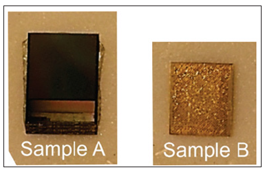
Figure 4:(a) Photomicrograph and (b) SEM image of dot pattern of Sample-A taken before putting the cover layer. (c) magnified photomicrograph and (d) unmagnified photomicrograph of dot patterns of Sample-B. Both are as supplied.

Figure 5:Experimental setup. Sample-A and Sample-B as mounted on the nanoscanner. Sample-A’ was also mounted the same way. These samples were scanned one at a time.
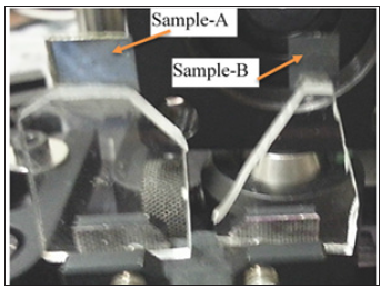
All samples were scanned over a small volume, one at a time. Built-in front end software interface was used for data acquisition via a suitable scanning protocol as described in Sec. 1.2, over selected areas and volumes of the chip. Figure 5 shows the samples as mounted on the nanoscanner. Measured reflectance, R, is a material dependent parameter, thus, also dependent on the position of the incident beam on the sample under measurement. This is because, the sample (e.g. the chips of the present study) is made of different materials arranged in different patterns; each having their own characteristic reflection. Thus, a 3D matrix of the position dependent reflected intensity is adequate for reconstructing an image of the volume via the aforementioned stratagem. Imaging of all samples was carried with identical protocol.
Results and Discussion
Sample-A
Figure 6:Two different views of 3D (volume) image of Sample-A, 100μmx100μmx20μm. The dot pattern is visible separated by blank semiconductor area seen as some grey lines.
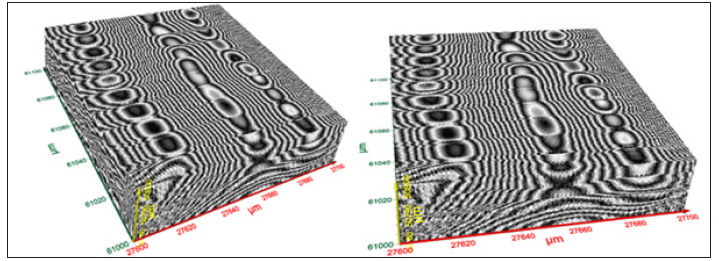
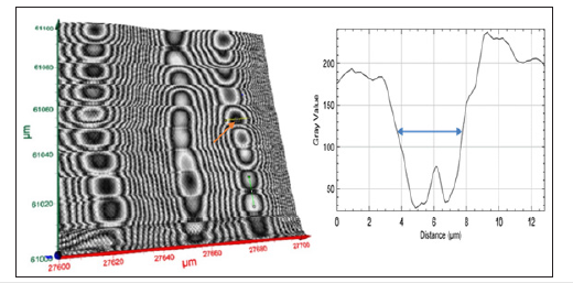
Figure 6 exhibits two different views of 3D image of Sample-A, over 100μm×100μm×20μm volume. The hidden dot pattern, below the top cover, has been revealed by the terahertz images. The rows of dots are separated by blank semiconductor area seen as some arbitrary grey line pattern because of some texture on the substrate. Since, the dot pattern is the objective for the present measurements, we neglect the arbitrary patterns and analyze the dot patterns only. Figure 7(a) shows the top surface extracted from Figure 6 for further analysis. Figure 7(b) shows a graphical analysis of Figure 7(a) along the cursor (yellow line). From this profile, dimensions of both the large and the small features may be quantified. Measured widths of two single dots are shown in Figure 8 as 2.7μm and 2.1μm, respectively. Figure 9 shows a graphical analysis of two other dots in a row along the cursor; the center-tocenter spacing for the given pair is ~4.0μm. However, it is seen that the dot spacing is not uniform; some are closer than others.
Figure 7:(a) Top surface extracted from 100μmx100μmx10μm volume. (b) Graphical analysis of Figure 7(a) along the yellow line. Profile of both large and small features may be quantified.

Figure 8:(a) Graphical analysis of a dot features. (b) the measured width of dot-A (left) is ~2.7μm and dot-B is ~2.1μm.
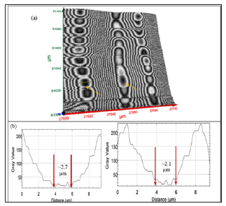
Figure 9:Graphical analysis of two dots in a row along the cursor; the dot spacing for the given pair is ~4.0μm. However, dot spacing is not uniform; some are closer than others.
Sample-B
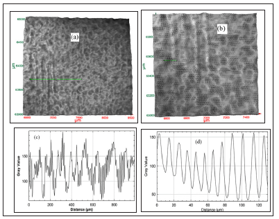
Figure 10(a) shows a wide area image of Sample-B over 2mm×2mm and Figure 10(b) exhibits a zoomed image of the same over 1 mm × 1 mm. Figure 10(c) shows a graphical profile of Figure 10(a) over the length of the cursor (see arrow) and Figure 10(d) exhibits a graphical profile of the image in Figure 10(b) across the cursor. From the graphical profile the size of a single dot was measured to be ~4.5μm (see arrow) at the FWHM. Unlike Sample-A, the dots on Sample-B are more uniformly spaced, as evident from the profile of Figure 10(d).
Figure 10:(a) Wide area image of Sample-B (2mmx2mm). (b) A close-up of approximately 1mmx1mm reveals fine dot pattern within bigger dots. (c) Graphical profile of (a) over the length of the cursor. (d) Graphical profile of (b) across the cursor. A single dot size at FWHM ~4.5μm.
Sample-A’
Figure 11 shows the analyses of Sample-A’ for the line pitch, i.e. distance between two consecutive lines (a) and (b) and the line width of a typical line (c) and (d). It is seen that typical line pitch is ~788nm and typical line width is ~190nm. Figure 12 exhibit a 3D view of the lines from which the line thickness (depth) was measured to be ~3.5μm. These numbers are compared with those obtained from SEM data in Table 1. From the 3D terahertz image (Figure 12), it was also revealed that the metal nano-lines have an aspect ratio along the thickness; i.e. the top thickness is slightly narrower than the bottom thickness. Only the present terahertz imaging is able to yield such 3D information; SEM or TEM are not able to produce such 3D perspectives. Figure 13 exhibits an example of layer-by-layer image analysis. Only 3 layers are shown on the XY plane. It is also seen from Figure 13 that individual layers are composed of nanograins; the size of individual grains may be measured by the same graphical analysis as before.
Figure 11:(a) line pitch (b) measured value of pitch is ~788nm (c) line width (d) measured value of line width is ~190nm.

Figure 12:Three-dimensional image of the metal lines on silicon substrate. An aspect ratio is observed across the thickness. The dimensional analysis is summarized in Table-1 along with the comparison with SEM data.
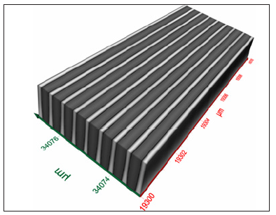
Figure 13:An example of layer-by-layer image analysis. Only 3 layers are shown on the XY plane. Here nanograins are visible.
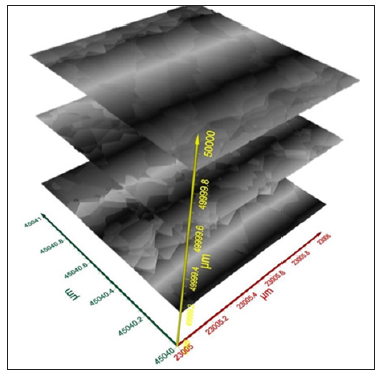
Table 1:Comparison between SEM and Terahertz results.

*The SEM data are as supplied by the vendor.
**%disagreement = ((new_value – original_value)/ABS(original_value))*100.
Conclusion
This paper demonstrates the camera-less non-destructive route of terahertz reconstructive imaging of features on semiconductor chips. Two different chips with different patterns were imaged and analyzed. Sample-A has a dot pattern that are hidden under the top cover. It was found that the dot pattern of Sample-A varied both in size and spacing; typical dot size is ~2.4μm and typical dot spacing is ~4μm. The dot pattern on Sample-B was relatively uniform; approximate size is 4.5μm. The surface imperfection of Sample-B was visibly identifiable. A third chip (Sample-A’) was also measured for the nano-scale lines analysis. The measured line width and line pitch are 190nm and 788nm, respectively; and the measured line depth was 3.5μm. These results agreed with the SEM results within the experimental error limits. The 3D terahertz image revealed that the metal nano-lines have an aspect ratio along the thickness; i.e. the top thickness is narrower, and the bottom thickness is wider. This 3D images are possible only from the present terahertz imaging technique; SEM or TEM are not able to produce similar 3D images. The technique of imaging presented herein is applicable to any kind of substrates and patterns including the semiconductor wafers and nanomaterials.
Acknowledgment
The authors wish to acknowledge partial support for this work by the Samsung Research Institute of Japan. Some concept of this paper was presented at the Semicon West 2018, Moscone South, Smart Manufacturing Pavilion, San Francisco, Thursday, July 12, 2018, 12:00pm-1pm.
References
- Abbe E (1873) Contributions to the theory of the microscope and the microscopic perception. Arch Mikrosk Anat 9(1): 413-468.
- Novotny L, Hecht B (2006) Propagation and focusing of optical fields, in principles of nano-optics, Cambridge U Press 3, UK, pp. 45-87.
- Rahman A, Rahman AK (2019) Nanoscale metrology of line patterns on semiconductor by continuous wave terahertz multispectral reconstructive 3-d imaging overcoming the abbe diffraction limit. In IEEE Transactions on Semiconductor Manufacturing 32(1): 7-13.
- Rahman A, Rahman AK (2014) Effective testing for wafer reject minimization by terahertz analysis and sub-surface imaging. ASMC.
- Rahman A, Rahman AK, Yamamoto T, Kitagawa H (2016) Terahertz sub-nanometer sub-surface imaging of 2D materials. J Biosens Bioelectron 7(3): 1-8.
- Rahman A, Rahman AK (2016) Terahertz spectroscopic analysis and multispectral imaging of epitaxially grown semiconductors with nanometer resolution. J Biosens Bioelectron 7(4): 1-6.
- Rahman A, Rahman AK, Tomalia DA (2017) Engineering dendrimers to produce dendrimer dipole excitation based terahertz radiation sources suitable for spectrometry, molecular and biomedical imaging. Nanoscale Horizons.
- Rahman A, Rahman A (2019) Sub-surface nanometrology of semiconductor wafers and graphene quality assessment via terahertz route. Proceedings of the ASMC.
- Davis JC (1986) Statistics and data analysis in geology. John Wiley and Sons, New York.
- Franke R (1982) Scattered data interpolation: Test of some methods. Mathematics of Computations 38(157): 181-200.
- Rahman A, Tomalia D (2018) Terahertz Based Nanometrology: Multispectral Imaging of Nanoparticles and Nanoclusters in Suspensions. Journal of Nanoparticle Research.
© 2019 Anis Rahman. This is an open access article distributed under the terms of the Creative Commons Attribution License , which permits unrestricted use, distribution, and build upon your work non-commercially.
 a Creative Commons Attribution 4.0 International License. Based on a work at www.crimsonpublishers.com.
Best viewed in


.jpg)





 Editorial Board Registrations
 Submit your Article
 Refer a Friend
 Advertise With Us

.jpg)



.jpg)








.bmp)
.jpg)
.png)
.jpg)





.jpg)


.png)

.png)


.png)


