- Submissions

Full Text
Novel Research in Sciences
Three Dimensional Lattice Imaging of Alumina Nanograins and Nanovoids Via Terahertz Multispectral Technique
Anis Rahman*
Applied Research & Photonics, USA
*Corresponding author:Anis Rahman, Applied Research & Photonics, USA
Submission: May 24, 2018Published: June 10, 2018
.jpg)
ISSN : 2688-836XVolume1 Issue1
Abstract
High purity alumina sample has been characterized via terahertz reconstructive lattice imaging technique. The camera-less technique uses a nanoscanner to create a digital three-dimensional representation of the sample via modified Beer-Lambert’s law, where, the reflected terahertz intensity is captured as a function of real coordinates on the sample of nanometer step size. This non-contact technique replaces the focusing lens and the focal plane array (e.g. a CCD) of a traditional camera which is limited by the Abbe diffraction limit. It was found that over a bigger area/volume, the generated images exhibit the amorphous nature of the alumina sample. However, when zoomed to a cubic micron volume, the nanograins are visible. The nanograins are more clarified in both the two-dimensional and threedimensional images upon further zooming, from which lattice parameters were quantified. Though the sample is comprised of nanograins, all grains are different in size and orientations, compared to each other. As such, while alumina is an amorphous material, it is composed of different kind of nanograins as revealed herein. A single nanograin was measured to be ~5.5nm. The lattice patterns within a nanograin are not identical either; indicating non-uniformity of lattice within a nanograin. In addition, nanovoids are also observed via layer-by-layer analysis. Two nanovoids were measured to be 2.78nm and 0.72nm, respectively. The technique is universal and may be applied to any material.
Introduction
High purity alumina bioceramics may serve as an alternative to surgical metal alloys for total hip prosthesis and tooth implants. The high hardness, low friction coefficient and excellent corrosion resistance of alumina offers a very low wear rate at the articulating surfaces in orthopedic applications [1]. Medical grade alumina has a very low concentration of sintering additives (<0.5 wt.%), very small grain size and a narrow grain size distribution. Thus, alumina is an inert biomaterial that is also a biodegradable material and well tolerated by the biological environment in human body. However, implant materials used in orthopedic surgery have exhibited some disadvantages, such as lack of direct chemical bonding and modulus mismatch between the implant materials and natural bone. The requirement of every bone analogue implant material is to mimic the biological and mechanical properties of the original bone. Current interest in orthopedic implants has come about in response to the original long-term follow-up studies of joint replacements [2].
In literature, there are information on various methods of synthesizing and characterizing alumina (Al2O3). Common techniques for characterization include electron microscopes (EM) such as SEM and TEM, and different spectroscopy [3-6]. While these techniques are effective and accurate, they are mainly destructive in nature. Nonetheless, the electron microscopy technique produces a frozen-in-time snapshot of a single surface; not to mention that it requires tedious and time-consuming sample preparation. Also, SEM/TEM images are often taken over very small areas to be able to see the details at higher magnification. Such a narrow area of observation is mandated by the focusing mechanism of the EM technique. Difficulties in noncontact atomic force microscopy (NCAFM) imaging have so far prevented high resolution imaging on surfaces of many insulators, most notably MgO and alumina [7]. Trace impurities and additives have long been known to strongly influence the fabrication and properties of alumina-based ceramics [8]. It is important to be able to inspect the whole specimen and/or as big an area as possible for the overall morphology of the microstructure/ nanostructure without sacrificing the ability to inspect the minute features on a nano-scale.
To this end, we are introducing a technique for 3D imaging with nano-meter resolution in a non-destructive mode, without limiting the sample size.
This terahertz multispectral reconstructive imaging technique [9] has virtually no sample preparation. Requirements of polishing the samples to electron transparency and of high vacuum have been eliminated. Details of the technique has been described elsewhere [9-11]. We have shown elsewhere [11] that breaking the Abbe diffraction limit (ADL) is a required condition but not sufficient for achieving nanometer resolution with terahertz waves where the wavelengths range from ~9 μm up to ~3000 μm. As described in [11], the reconstructive imaging technique utilizes a nano-scanner in conjunction with a modified Beer Lambert law to create a 3D data matrix of the sample under test (SUT). Thus, compared to a charge coupled device (CCD) based imaging camera, where a lens is used for focusing an object’s image on the CCD, the reconstructive imaging utilizes a nanoscanner for digitizing an object’s terahertz response in terms of the reflected intensity of the entire volume [11]. That is, the scanning sequence scans a surface line by line where the scanning pitch is chosen by the user within the limits of the positioning stages used by the nanoscanner. A volume is divided into a number surfaces and scanning is repeated for all surfaces in sequence to reconstruct the volume. An algorithm called the “inverse distance to power equation,” [12,13] is used to create a 3D lattice from the measured data. Finally, a suitable color rendering of the lattice is used for producing the image.
Experimental Methods and Material
The setup used for the current investigation is able to define a step size of ~24.83 nm for the highest resolution and >1 mm for the lowest resolution. The above-mentioned algorithm interpolates and reproduces features with a resolution of <1 nm. As we have reported recently [11], achieving an image resolution of ~1 nm using terahertz radiation requires overcoming the Abbe diffraction limit and a stratagem for high resolution image generation [14]. A piece of polished alumina plate (Figure 1) was used for the current investigation. Approximately, 4×2×3 μm3 volume was scanned at the highest resolution. The images and their analyses are presented in Figures 2-8.
Figure 1:A piece of alumina plate used for the present study.
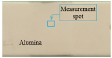
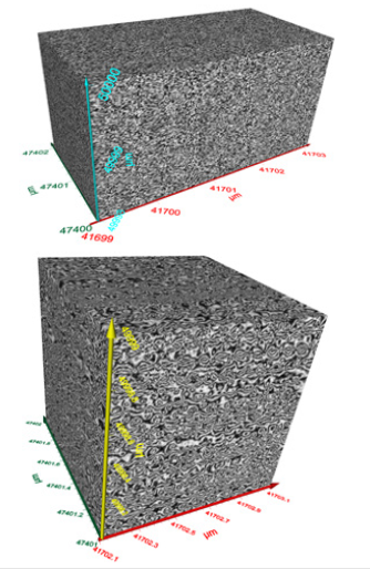
Figure 2:Three-dimensional (3-D) images of alumina. (a) over bigger area of 4×2×3 μm3 it looks totally amorphous. (b) Zoomed over 1 cubic micron volume; some structures are visible.
Results and Discussion
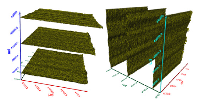
Figure 2 exhibits three-dimensional (3-D) images of alumina; 2 (a) is an image over a bigger volume of 4×2×3 μm3. From this wider image, the sample looks totally amorphous. When zoomed closer to 1 cubic micron volume; (see 2 (b)), some structures are visible. The structures are quantified via lattice scale zooming, as explained below. Figure 3 displays high resolution images of 50 cubic nanometer volume; 3D views from 4 different angles are shown. Here, nanograins are visible. This is more clarified in the two-dimensional (2-D) images exhibited in Figure 4 for three different slices (each 50 nm × 50 nm), extracted from Figure 3. Although the nanograins are clearly visible; however, all grains are different than each other. As such alumina is an amorphous material. In contrast, for example, metallic lattice is expected to be continuous [15, 16] while semiconductor lattice may have stacking fault and dislocations [16]. Figure 5 display another slice of 50 nm × 50 nm image, where, nanovoids are visible at the lower left corner. Two nanovoids are quantified in Figure 6 along the horizontal direction. The nanovoid marked ‘A’ (Figure 6 (a)) has a dimension of ~2.78 nm, while the one marked ‘B’ (Figure 6 (b)) has a width of 0.72 nm. Both of these nanovoids are of irregular shapes; therefore, the dimensions are different in the vertical direction (not shown). Figure 7 exhibit a different slice of 50 nm × 50 nm image; here the nanograins are clearly visible. It is seen that all nanograins are of different size and different crystalline orientation; none are identical. For example, a nanograin at the cursor (yellow line, see arrow marked A) has a measured dimension of ~5.5 nm. The lattice spacings of this particular grain are not uniform either, as shown in Figure 8. The same is true for all other nanograins. An observation here is that within some grains, dislocations are clearly visible; see for example, arrow marked B in Figure 7. Figure 9 exhibits an example of layer-by-layer analysis over 1 μm × 1 μm area. Figure 9 (a) shows three non-adjacent image slices on the XY plane, some differences in the slices are notable. Figure 9 (b) exhibits three nonadjacent image slices on the XZ plane. Position of all slices are as indicated by the respective axes.
Figure 3:High resolution image of 50 cubic nanometer volume. 3D views from 4 different angles.

Figure 4:Three different surface images (50 nm x 50 nm) extracted from Figure 2. Nanograins of different orientations and sizes are visible. Each nanograin exhibits its own structure.
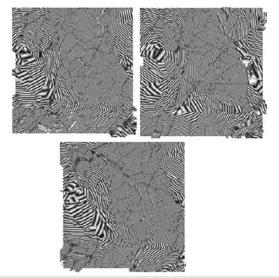
Figure 5:Two nanovoids seen (marked A & B). There dimensions are shown below.
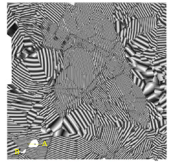
Figure 6:Quantification of the nanovoids of Figure 4. Void A is ~2.78 nm and void B is ~0.72 nm.
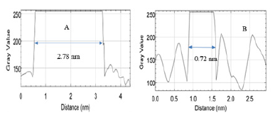
Figure 7:Nanostructure of single side from Figure 2 is used for grain size quantification. The nanograin at the cursor (see arrow A) has a measured dimension of ~5.5 nm. Within some grains, dislocations are clearly visible; see for example, the grain indicated by arrow B.
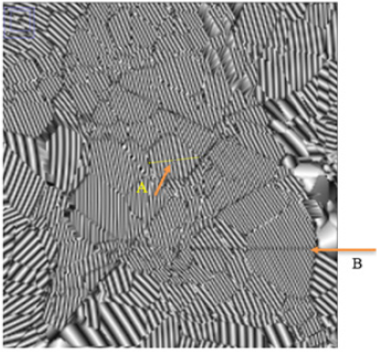
Figure 8:Quantification of a nanograin’s lattice size. The lattice spacings within the nanograin are not uniform.
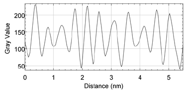
Figure 9:An example of layer-by-layer analysis over 1μm×1μm area. (a) three non-adjacent image slices on the XY plane, (b) three non-adjacent image slices on the XZ plane. Position of the slices are as indicated by the axes
Conclusion
An alumina sample has been characterized by means of terahertz reconstructive lattice imaging technique. The camera-less technique uses a nanoscanner to create a digital representation of the sample via modified Beer-Lambert’s law, where the reflected terahertz intensity is captured as a function of actual position on the sample. Thus, this non-contact technique replaces the focusing lens and the focal plane array (e.g. a CCD) of a traditional camera imaging, which is limited by the Abbe diffraction limit, by a smart nanoscanner and computer algorithm for high resolution image generation with bigger wavelengths. For the alumina sample of the present study, it was found that over a bigger area/volume, the images exhibit the amorphous nature of the sample. However, when zoomed to a higher resolution, nanograins of different shapes and sizes become visible. Therefore, while alumina is an amorphous material, it is composed of different kind of nanograins as revealed herein. Some nanograin’s measured to be ~5.5 nm; others are bigger but there are also grains smaller than 5 nm. The lattice patterns within a nanograin are not uniform; thus, indicating the presence of lattice planes’ contraction and dilation within a single nanograin. Additionally, nanovoids are also observed via layerby- layer analysis. Two nanovoids were measured to be 2.78 nm and 0.72 nm, respectively. The technique is universal and may be applied to any materials.
References
- Cordingley R, Kohan L, Ben Nissan B, Pezzotti G (2003) Alumina as an Orthopaedic Biomaterial Characteristics, Properties, Performance and Applications. Journal of the Australasian Ceramic Society 39(1): 20-28.
- Karlssona M, Palsgard E, Wilshaw PR, Di Silvio L (2003) Initial in vitro interaction of osteoblasts with nano-porous alumina. Biomaterials 24(18): 3039-3046.
- Hartmann S, Sachse A, Galarneau A (2012) Challenges and strategies in the synthesis of mesoporous alumina powders and hierarchical alumina monoliths. Materials (Basel) 5(2): 336-349.
- Leenaars AFM, Keizer K, Burggraaf AJ (1984) The preparation and characterization of alumina membranes with ultra-fine pores. J Mater Sci 19(4): 1077-1088.
- Wunderlich W, Padmaja P, Warrier KGK (2004) TEM characterization of sol-gel-processed alumina-silica and alumina-titania nano-hybrid oxide catalysts. Journal of the European Ceramic Society 24(2): 313-317.
- Xinhua Lin, Yi Zeng, Soo Who Lee, Chuanxian Ding (2004) Characterization of alumina-3wt.% titania coating prepared by plasma spraying of nanostructured powders. Journal of the European Ceramic Society 24(4): 627-634.
- Foster AS, Rohl AL, Shluger AL (2001) Imaging problems on insulators: What can be learnt from NC-AFM modelling on CaF2? 72(1): S31-S34.
- KL Gavrilov, SJ Bennison, KR Mikeska, R Levi Setti (1999) Grain boundary chemistry of alumina by high-resolution imaging sims. Acta mater 47(15-16): 4031-4039.
- Rahman A, Rahman AK, Yamamoto T, Kitagawa H (2016) Terahertz sub-nanometer sub-surface imaging of 2D materials. J Biosens Bioelectron 7: 3.
- Rahman A, Rahman AK (2016) Terahertz spectroscopic analysis and multispectral imaging of epitaxially grown semiconductors with nanometer resolution. J Biosens Bioelectron 7: 4.
- Rahman A, Rahman AK (2018) Nanoscale metrology of line patterns on semiconductor by continuous wave terahertz multispectral reconstructive 3-D imaging overcoming the abbe diffraction limit. IEEE Transactions on Semiconductor Manufacturing 32(1): 7-13.
- Davis JC (1986) Statistics and data analysis in geology. John Wiley and Sons, New York, USA.
- Franke R (1982) Scattered data interpolation: test of some methods. Mathematics of Computations 38(157): 181-200.
- Abbe E, Arch. Mikrosk. Anat. 9, 413 (1873) also cited in Lipson, Lipson and Tannhauser (1998). Optical Physics, Cambridge, United Kingdom, p. 340.
- Anis Rahman, Rahman AK (2019) Sub-surface nanometrology of semiconductor wafers and graphene quality assessment via terahertz route. ASMC 2019 proceedings.
- Anis Rahman (2017) Terahertz multispectral imaging of epitaxially grown semiconductors’ lattice defects. ASMC 2017 proceedings.
© 2019 Anis Rahman. This is an open access article distributed under the terms of the Creative Commons Attribution License , which permits unrestricted use, distribution, and build upon your work non-commercially.
 a Creative Commons Attribution 4.0 International License. Based on a work at www.crimsonpublishers.com.
Best viewed in


.jpg)





 Editorial Board Registrations
 Submit your Article
 Refer a Friend
 Advertise With Us

.jpg)






.jpg)





.bmp)
.jpg)
.png)
.jpg)



.jpg)


.png)

.png)


.png)


