
- About Us
- Information
-

The Author ensures that the research has been conducted responsibly and ethically with adherence to all relevant regulations. read more..
- For Authors
- For Reviewer
- Manuscript Guidelines
- Membership
- Publication Ethics
-
- Journals
- Reprints
- e-Books
- Videos
- Policies
- Contact Us
 COVID-19
- Submissions


Full Text
Determinations in Nanomedicine & Nanotechnology
Estimation of The Lattice Parameters, Crystallite Size and Internal Micro Strain of Cu1-Xinxse2 Thin Films by Williamson-Hall Method
Alaa Ahmed Saad Akl*
Faculty of Science, Saudi Arabia
*Corresponding author:Alaa Ahmed Saad Akl, Faculty of Science, Saudi Arabia
Submission: December 16, 2019;Published: February 20, 2020

ISSN: 2832-4439 Volume1 Issue5
Abstract
In this work, Cu1-xInxSe2 thin films have been grown on heated glass substrates using chemical spray pyrolysis. Characterizations and compositional analysis of Cu1-xInxSe2 thin films were obtained by X-ray Diffraction (XRD) and Electron Dispersion Analysis (EDX). Microstructure parameters as a function of Cu/In and the substrate temperature (Tsub) in the range of 548K to 623K have been study. Williamson-Hall method has been used to determine the crystallite size, microstrain. XRD revealed that a polycrystalline CuInSe2 thin films with the hexagonal structure having preferential growth along the <002> direction. At the Cu/In ratio increased, improved of the degree of crystallinity and decrement of both, the lattice parameters and volume of unit cell. Also, the crystallite size was found to be increased and decreased with the growth temperature. On the contrary, the microstrain values were decreasing with the growth temperature and Cu/In ratio were increasing.
Keywords: Spray pyrolysis; X-ray diffraction; CuInSe2 thin films
Introduction
Copper Indium di-Selenide (CIS) is one of the most promising semiconductor materials used in solar cells in recent years due to its favorable electrical and optical properties, durability and cost-effectiveness [1-5]. CuInSe2 is a member of the I-III-VI2 semiconductor group and is present in the chalcopyrite phase of the zinc blende family [4]. Various methods such as Molecular Been Epitaxial (MBE) [6], flash vaporation [7,8], multi-source evaporation [9], single-source evaporation [10], RF-sputtering [11], spray pyrolysis [12,13], Chemical precipitation [14] and Stacked Elemental Layer (SEL) [15,16] were developed to synthesize CuInSe2 thin films.
The Photovoltaic behavior (PV) of thin film heterogeneous solar cells dependent on the CIS is largely dependent on their structural properties. It has been found that CIS thin films have a disordered / ordered structural phase, depending on growth conditions. The hetero junctions’ complications formed from the required phase show a good conversion (PV), while the disordered phase shows a very weak response. Therefore, the film growth conditions must be adjusted so that CIS composite films that correspond to the required phase allow good conversion (PV). The nature of the direct band gap (1.04eV) and the high absorption coefficient (5x105cm-1) [9,13] ensure the aggregation efficiency to be relatively independent of the diffusion length of minority carriers. Among these methods, the pyrolysis of chemical spray that presents a gentle, simple and economical method with the advantage of allowing patterned crystal growth and control is demonstrated by the crystallization engineering control feature of CuInSe2 films of large area. The thin films prepared in this method may not be of high quality but are suitable for studies conducted in this work. In this method, it is also possible to prepare mixed thin films of two or more compounds where the mixing is ideal as the compounds are mixed in the forms of their solutions. The chemical spray pyrolysis method is also suitable for preparing doping thin films, as the ratio of doping can be determined very accurately [13-20].
The aim of this study was to prepare Cu1-xInxSe2 thin films using chemical spray pyrolysis technique to design process equipment as well as to determine the experimental conditions necessary to produce stoichiometric of CuInSe2 films. The effect of growth temperature and Cu/In ratios on parameters of microstructure was studied.
Experimental
Copper-grade chloride reagent (CuCl2), indium chloride (InCl3) and N-N dimethyl seleno Urea (N-N-DMSeU) were used to prepare a spray solution that forms CuInSe2 films on glass substrates. Stock solutions were prepared 0.025M from CuCl2,0.0625M from InCl3 and 0.165M from N-N-DMSeU. A large portion of these solutions were diluted with a fixed amount of ethyl alcohol (25ml) and Deionized water (DI) (100ml) as a final concentration of 5x10⁻⁴M. The solution volumes in InCl3 and DMSeU remained constant at 1.00ml and 1.25ml, respectively, while the volume of CuCl2 solution ranged from 2.25ml to 2.7ml to obtain a stoichiometric ratio 0.9: 1: 3.3 to 1.1: 1: 3.3. The starting solution was prepared just before the spray began. This solution was passed through airless spray with a nozzle diameter of 0.7mm. The spray process lasted for 15 seconds. The interval between spraying was about 3 minutes. This period is sufficient to avoid excess cooling of glass substrates. The pH of the solution was maintained constant at 2.35 by adding hydrochloric acid. The spray rate used was 70ml/hr with a pre-modified peristaltic pump. The nitrogen flow rate remained constant at 80mL/h by a regulator connected to the nitrogen bottle. The temperature controller was used to measure the growth temperature and control the resistance heater through thermocouples. To prevent DMSeU dissociation in primary selenium, all spray deposits were made in a dark room.
The film thickness of the prepared samples remained constant during all precipitation processes at 500nm and was measured using a Fizeau multi-beam fringes upon reflection using either white light or monochromatic light. The colored interference fringes enabled the determination of the order of magnitude of the fringes shift, while the monochromatic edges change when part of the arrangement separation was measured using an eyepiece micrometer. To investigate the film structure, a JEOL X-ray diffraction meter (model JSDX-60PA) operating at 40kV and 35mA using the Cu-Kα radiation filtered by Ni was used to obtain diffraction patterns. Continuous scanning was applied with a slow scan speed (1°/min) and time constant for detector is 1sec. A range of 2θ was scanned from 6° to 72°. So that all possible diffraction peaks can be discovered. Polycrystalline defect free silicon powder was used for instrumental correction. Compound chemical analysis of current samples was studied using energy dispersion analysis in X-ray spectroscopy, EDX (model Oxford instruments, England).
Result and Discussion
XRD analysis
XRD patterns of Cu1-xInxSe2 films deposited on heated glass substrates appear at different growth temperature and Cu/In ratio are shown in Figure 1-3. These patterns were studied in a comprehensive study to determine the expected phases such as the free elements (Cu,In,Se), the binary and/or ternary phases the compounds of these elements and their oxides. It was found that all samples, regardless of the state of preparation, show four major peaks that appear at 2θ=26.64, 44.22, 52.54° and 70.92° have a corresponding (112), (204,220), (116,332) and (316,332). Also, the beaks of the manor are a subsidiary one that appeared at the diffraction angles of 13.24° and 24.26°.
Figure 1: The x-ray diffractogram of Cu1-xInxSe2 thin films deposited at 548K with different Cu/In ratios ranging from 0.90 to 1.10.

Figure 2: The x-ray diffractogram of Cu1-xInxSe2 thin films deposited at 573K with different Cu/In ratios ranging from 0.90 to 1.10.

Figure 3: The x-ray diffractogram of Cu1-xInxSe2 thin films deposited at 623K with different Cu/In ratios ranging from 0.90 to 1.10.

The sequence and intensity of the major peaks are (112), (204,220), (116,312) and (316,332), corresponding to CuInSe2 phase with a tetragonal structure according to PDF number 80-0535. Obviously, the spectra are free of additional peaks that arise from phases, elemental, binary or ternary phases. Therefore, it was concluded that the films obtained were actually tetragonal chalcopyrite CuInSe2. XRD intensities peaks and FWHM vary according to preparative conditions, but they still have the same positions. In addition, the observed high intensity of the reflection from (112) indicates the preferred orientation along the direction <112>. The calculated ratio I112/I204 for the films investigated is greater than 2.5 in all setting conditions. It has been found that in literature [8-24] for random orientation, this ratio should be ≈1.5. This means that prepared samples are preferentially oriented along <112> direction. Additionally, the two conjugated peaks appeared at 2q=13.24° and 2q=24.26° that marked Cu2-xSe and observed cubic structure. The lattice parameter of Cu2-xSe increases rapidly from a=5.741±0.02Ǻ for the newly formed phase reaching = 5.833±0.02Ǻ at 623K.
Thus, the obtained chalcopyrite phase for prepared films is independent of both growth temperature and Cu/In ratios (0.9 to 1.1). Therefore, the effect of these parameters is on the microstructure, lattice parameters and their preferential direction is negligible. Where the average of lattice parameters a and c of the ternary compound CuInSe2 of Cu/In a ratio are determined as a=5.7809±0.02Ǻ and c =11.5565±0.04Ǻ; respectively. Which closely align with the value given in PDF No. 80-0535. These values are slightly less than those reported for single crystal of CuInSe2.
Influence of Cu/In on the lattice parameters
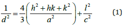
Based on a careful study of the XRD planes in a different Cu/In ratio, one can notice that a slight shift has occurred towards the higher 2θ values. It can be seen that line (112) has been shifted from angle 26.60° to 26.80° and line (204/220) has been shifted from 44.22° to 44.40°; respectively. Moreover, CuInSe2 of hexagonal structure has lattice constants a and b equal to 5.781Å and co = 11.552Å, corresponding to PDF cards No. 80-0535. Consequently, the shift in the position of X-ray diffraction lines can be attributed to the introduction of a copper ion that has a small ionic radius at interstitial distances between In and Se ions in the CuInSe2 unit cell. Thus, it will cause this observed little shift in the position of X-ray diffraction planes. On the other hand, the interplanar spacing value, d, is calculated from the Bragg's law (nλ = 2d sinθ), while the lattice constants (a) and (c) can be calculated from a lattice geometry formula for hexagonal structure, which are given as follows [25,26]:
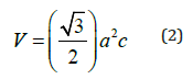
Therefore, and knowing the values of (a) and (c), anyone can be calculated the lattice volume (V) of the unit cell of CuInSe2 samples using this simple equation [25,27]:
When the values of d were calculated, they were found to decrease slightly with the addition of more copper to the in account, for all diffraction lines. This may be due to the smaller bonding energy value of the Cu-In bonding than that in the In-Se bonding, as these bonding energies measure bond strength and attractive forces between the sample components. Figure 4a-4c are shown as variance of the lattice parameters and volume of unit cell in different Cu/In ratio and growth temperatures.
Figure 4a: The lattice parameters, a=b (Å) as a function of Cu/In ratio at different growth temperatures.

Figure 4b: The lattice parameters, c(Å) as a function of Cu/In ratio at different growth temperatures.

Figure 4c: The volume of unit cells as a function of Cu/In ratio at different growth temperatures.

Obviously, calculated values were found for the lattice parameters and volume of unit cell, where the outward lattice relaxation is less than 1.7% around the interstitial, and greater (up to 3.5%) but more internal relaxation about the vacancy. Specifically, the original Cu-Se bond length of 2.40 °C increases to 2.60 °C (between interstitial Cu and its closest neighbors to the Se region). Also, the length of the In-Se bond is 2.60° to 2.65° (relative to interstitial copper atoms). Around the Cu vacancy, the lattice experiences a contraction: the edge of the Se tetrahedron around a Cu site changes from 3.84-3.97Å in the perfect crystal to 3.53-3.62Å for the case of missing Cu. The total energy of a system with displaced Cu atom is by merely 3eV higher than in the perfect crystal [28]. The almost exact agreement with experimental lattice parameters might be accidental for CuInSe2, but anyway it is a good indication that pseudo potentials and basic functions are appropriately chosen. The c/a ratio remains very close to 2.0 in the chalcopyrite structure CuInSe2, as was the case in both experiment and earlier studies; moreover, the most accurately in all cited calculations.
Preferred orientation and texture coefficient, TC
A preferred orientation is a positive direction within the texture of the material that arises as a result of the material having a strong tendency to crystallize in a particular direction. If the sample had a texture coefficient value equal to unit (TC (hkl)=1), then the crystals of that sample were randomly directed. Whereas if the sample contained TC>1, its crystals were directed in a specific (hkl) direction [28-31]. The higher the value of TC, the more crystals that periodically oriented. This coefficient can be obtained using the following equation [28,32-34]:
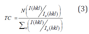
Where I(hkl) is the intensity that is experimentally determined for a given plane, while Io(hkl) is the standard intensity obtained from PDF cards that corresponds to the same plane (hkl). N is the total number of reflections and n is the number of diffraction peaks [29]. The calculated values for this coefficient for the three main diffraction lines are included in Table 1. It was noted that the diffraction line (112) with a greater intensity (I) contains the largest TC value among other lines of the current CuInSe2 samples. This means that the plane (112) of the chalcopyrite structure of CuInSe2 samples is the appropriate plane for the growth of small crystals with the lowest surface energy. However, the value of TC should decrease as the growth temperature increases from 1.326 to 1.104. This means that this plane is the preferred plane for all Cu/In ratios. It was also noted that the lines (204/220) and (116,312) have the lowest intensity and have a smaller TC value. Similar results were obtained by other authors in the previous literature [31,35].
Table 1: The calculated values of texture coefficient, TC of Cu1-xInxSe2 at different growth temperature and Cu/In ratio is 1:1.

Determination of the microstructural parameters
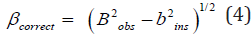
For all samples prepared from Cu/In ratios at different growth temperatures, the estimated correct integral breadth (β) of the X-ray diffraction lines detected by the area under the beak divided by the maximum intensity (Io) was calculated. The correct integral broadening of any sample examined (β) is somewhat resulted by subtracting two factors, the observed broadening, B and the instrumental broadening, b. An integral breadth of the peak of XRD was used to estimate the correct broadening of the synthesized CuInSe2 samples [36,37]. There is more than one peak treatment, such as Lorentzian and Gauss distribution treatments. According to the Gaussian distributions, the correct broadening of the investigated sample is given as follows:
A qualitative description for operative is provided based on profile shape variation. Finally, the exact mean stress and change with coherence length in terms of stress derivatives and local strain were finally explained to extract information regarding the nature of stress confinement in crystals. The Williamson Hall method was used to obtain the average crystallite size and internal microstrain. This is one of the most favorite methods, especially for samples with many X-ray diffraction peaks. The mathematical equation is as follows [28,36,38,39]:
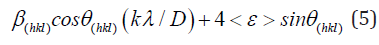
Where β(hkl) is the estimated correct broadening of the sample, θ(hkl) is the diffraction angle, k is the shape factor and, in our case, it is equal to 0.94. X-ray wavelength, λ equals 0.154184nm, D is the average crystallite size and <ε> is the average fine internal microstrain. Equation (5) of Williamson-Hall method extended the correct pure peak broadening of the sample as it is the sum of the contributions of both the crystallite size and the exact microstrain that may be present in the sample (Table 2). They assumed that the exact microstrain presented in the sample was uniform, that is, they considered that the sample had an isotropic nature. Thus, from equation (5), if a graph is drawn between (β cos θ) on the y-axis vs. (4 sin θ) on the x-axis, a straight line is obtained [28]. From the intercept part and slope, it can calculate the average of crystallite size of the crystals, D and the exact average internal microstrain <ε>, respectively. Figure (5-7) represents the plotted of (β cos θ) versus (4sin θ) for the current CuInSe2 samples at different growth temperatures. Four diffraction planes were used to calculate and draw the curves (112), (204), (116) and (316) that characterize the XRD of the prepared samples. Figure 8 shows the estimated crystallite size as a function of the Cu/In ratio at different growth temperatures and is tabulated in Table 3.
Table 2: The average values of crystallite size (nm) with different of Cu/In ratios of Cu1-xInxSe2 films.

Table 3: The average values of microstrain with different of Cu/In ratios of Cu1-xInxSe2 films at different growth temperature.

Figure 5: Determined the crystallite size and microstrain of Cu1-xInxSe2 as a function of Cu/In ratio at growth temperature of 548K by Williamson-Hall's method.

Figure 6: Determined the crystallite size and microstrain of Cu1-xInxSe2 as a function of Cu/In ratio at growth temperature of 573K by Williamson-Hall's method.

Figure 7: Determined the crystallite size and microstrain of Cu1-xInxSe2 as a function of Cu/In ratio at growth temperature of 623K by Williamson-Hall's method.

Figure 8:

Figure 9:

Clearly, the size of the crystals increases with the increase in Cu/In ratio and growth temperature. This means that growth under rich copper conditions seems favorable to obtain a large of crystallite size. On the other hand, increasing indium content lowers the size of crystals and reduces the precipitation rate. Similar behavior to the difference in crystallite size between the In-rich and Cu-rich of CuInSe2 thin films has been reported in the literature [13,14,40]. Figures 9; Table 3 Show changes in the internal microstrain of CIS films as a function of the Cu/ In ratio. It is evident that the microstrain increases with increasing Cu/In ratio or growth temperature, either as expected from the atoms, or the ions are ejected from the target source by transporting higher momentum due to ionic collisions. The higher the temperature or the ratio of Cu/In leads to an increase in the kinetic energy of the ions during deposition on the substrate and consequently an increase in the amount of mobility and collisions between the ions so the internal microstrain increase during the formation of the compound CuInSe2
EDX and the elemental composition analysis
Table 4: The elemental composition ratios (atomic and weight percentage) of investigated samples are indicated in atomic percent Cu: In: Se.

The energy dispersive analysis of X-ray or energy dispersive X-ray spectroscopy technique (EDAX, EDX or EDS) is considered a powerful tool used to analyze the elemental constituents of any chemical compound contains more than one element. The elemental composition analysis of the present CuInSe2 samples was examined, thereby the weight and atomic percentages of copper, indium and selenium elements were obtained [40]. Table 4 gives typical compositions of Cu1-xInxSe2 thin films prepared by spray pyrolysis at different Cu/In ratios. Generally, the elemental analysis using the EDX spectrometer may give an assessment of the sample about 0.1%. Generally, there is a good agreement between the theoretical calculated ratios and those obtained experimentally.
Conclusion
Cu1-xInxSe2 thin films have grown at different growth temperatures and vary of the Cu/In ratios preparation by spray pyrolysis technique. It has been observed that the microstructure depends on the preparation conditions, especially the growth temperature and the Cu/In ratios. Single phase CuInSe2 thin films are obtained with chalcopyrite structure regardless of the change in Cu/In ratio and growth temperature from 0.9 to 1.1 and 548K, 573K and 623K, respectively. The crystallite size increases with the increase in Cu/In ratio and growth temperature. This means that growth under Cu-rich conditions seems favorable to obtain a large size of crystals. By adjusting the spray parameters, thin films of CIS with a chalcopyrite structure and <112> preferred direction can be obtained. In addition, the size of the crystals was increased by adding more copper element due to the crystallization of small crystals and the reduction of free volumes at the boundaries, which support the results obtained from XRD. Therefore, the increase in copper richness improves the nature of crystallization of samples and reduces the parameters of the crystal lattice and the unit cell size. Moreover, we found the value of internal microstrain to increase with increasing both the Cu/In ratio and the growth temperature. This is due to the fact that ions exit from the spray nozzle towards the surface of the substrate with high momentum and high kinetic energy, increasing the chance of collisions between ions during precipitation and thus increasing internal stress pressure during the process of forming the ternary compound of CuInSe2.
References
- Kazmerski LL, White FR, Morgan GK (1976) Thin‐film CuInSe2/CdS heterojunction solar cells. Appl Phys Lett 29(4): 268.
- Shay JL, Wagner S, Kasper HM (1975) Efficient CuInSe2/CdS solar cells. Appl Phys Lett 27(2): 89.
- Samaan ANY, Vaidhyanathn R, Noufi R (1986) Solar cells, p. 16181.
- Hovel HJ (1976) Semiconductors and semimetals. 29(11): 85.
- Moorthy SB, Dhanasekaram R, Ramasamy P (1991) Thin solid films, pp. 198209.
- Salviati G, Seuret D (1983) Thin solid films, pp. 104.
- Noufi R, Mason A, Franz A (1991) Thin solid films, p. 202-299.
- Parkes J, Tomlinson RD, Hampshire MJ (1973) Crystal data for CuInSe2. J Appl Cryst 6: 414-416.
- Cullity BD (1978) Elements of x-ray diffraction. (2nd edn) USA, pp. 102.
- Scheer R, Diesner K, Lewerenz HJ (1995) Experiments on the microstructure of evaporated CuInS2 thin films. Thin solid films 268(1-2): 130-136.
- Arraud MC, Ouchen F, Martin L, Duchemin S (1998) CuInSe2 thin films grown by MOCVD: Characterization, first devices Thin Solid Films 324(1-2): 115-123.
- Subbaramaiah K, Sundara RJ (1992) Thin solid films 208: 247.
- Alaa AA, Afify HH (2008) Materials Research Bulletin 43: 1539.
- Zouaoui A, Lachab M, Hidalgo ML, Chaffa A, Llinares C, et al. (1999) Thin solid films 339: 10.
- Tuttle JR, Albin DS, Noufi R (1991) Thoughts on the microstructure of polycrystalline thin film CuInSe2 and its impact on material and device performance. Solar Cells 30(1-4): 21-38.
- Akl AA (1997)El-Minia University, Egypt.
- Zouaoui A, Lachab M, Hidalgo ML, Chaffa A, Llinares C, et al. (1999) Thin solid films 339: 10.
- Subbaramaiah K, Sundara RV (1992) Thin solid films 208: 247.
- Shirakata S, Terasako T, Kariya T (2005) J Phys Chem Solids 66: 1970.
- Beck ME, Cocivera M (1996) Thin solid films 272: 71.
- Alaa AA, Mahmoud SA, Shomar SMA, Hassanien AS (2018) Materials Science in Semiconductor Processing 74C: 183-192.
- Barret CS, Massalski TB (1980) Structure of metals pergamon press. Oxford, UK.
- Ilican S, Caglar Y, Caglar M (2008) Polycrystalline indium doped ZnO thin films: Preparation and characterization. J Optoelectron and Advanced Materials 10(10): 2592-2598.
- Chouikh F, Beggah Y, Aida MS (2011) J Mater Sci Mater Electron 22: 499-505.
- Khorsand Z, Majid WHA, Abrishami ME, Ramin Y (2011) Solid State Sciences 13: 251.
- Cullity BD (1979) Elements of X-Ray Diffraction. In: Postnikov AV, Yakushev MV (Eds.), Thin solid films pp. 451-452.
- Postnikov AV, Yakushev MV (2004) Thin solid films. 141: 451-452.
- Singh HL Vishwa K (2015) Materials Science Poland. 33(4): 751.
- Eid AH, Seddek MB, Salem AM, Dahy TM (2009) Vacuum 83: 401.
- Caglar Y (2013) Journal of Alloys and Compounds 560: 181
- Singh BK, Tripathi S (2016) J Mater Sci: Mater Electron 27: 2360.
- Alaa AA, Hassanien AS (2014) Inter J Advanced research 2(11): 1.
- Alaa AA, Hassanien AS (2015) Superlattices and microstructures 85: 67.
- Alaa AA, Hassanien AS (2015) Physica: B 473: 11.
- Yakushev MV, Mudryi AV, Gremenok VF, Zaretskaya EP, Zalesski Y, et al. (2004) Thin solid films 133: 451-452.
- Alaa AA, Ashour A, Ramadan AA, Hady KAE (2001) Vacuum 61: 75.
- Ashour A, Alaa AA, Ramadan AA, Hady KAE (2004) Thin solid films, p. 467300.
- Cullity BD (1979) Addison-Wesley Publishing Company, Boston, USA.
- Yogamalar R, Srinivasan R, Vinu A, Ariga K, Bose AC (2009) X-ray peak broadening analysis in ZnO nanoparticles. Solid State Communications 149(43): 1919-1923.
- Moharrama AH, Harzb MM, Salemc A (2001) Applied Surface Science 172: 61.
© 2020 Alaa Ahmed Saad Akl. This is an open access article distributed under the terms of the Creative Commons Attribution License , which permits unrestricted use, distribution, and build upon your work non-commercially.
Editor In Chief


.jpg)


Signup for Newsletter

Quick Links
 Editorial Board Registrations
 Submit your Article
 Refer a Friend
 Advertise With Us
Our Recent Edition

.jpg)


Top Editors


.jpg)


.bmp)
.jpg)
.png)
.jpg)


.jpg)


.png)

.png)


.png)


Financial Support

Sponsors

Latest e-Books

Latest Video

 a Creative Commons Attribution 4.0 International License. Based on a work at www.crimsonpublishers.com.
Best viewed in
a Creative Commons Attribution 4.0 International License. Based on a work at www.crimsonpublishers.com.
Best viewed in