- Submissions

Full Text
COJ Technical & Scientific Research
Low-Resistance Ohmic Contact Materials for p-GaN Based on Metallurgy
Yasuo Koide*
National Institute for Materials Science (NIMS), Japan
*Corresponding author:Yasuo Koide, National Institute for Materials Science (NIMS), Japan
Submission: April 27, 2023; Published: May 16, 2023

Volume4 Issue2May , 2023
Abstract
A guideline for development of low-resistance Ohmic contact materials is to form Intermediate Semiconductor Layers (ISLs) with high dopant concentration or low energy barrier (φB) at the metal/ semiconductor interface by metallurgical reactions. For n-GaAs, Ge in AuNiGe and In in NiInW are found to play an important role in forming these ISLs. For p-GaN. In is a candidate element to form ISL with low φB p-type ISL, but a method to form ISL metallurgically has not been discovered yet. On the other hand, as a specific phenomenon, thermal annealing in oxygen ambient and metal/InSnO contact has been found to be effective in reducing the contact resistivity. Oxygen plays an essential role in the metallurgical reaction, but its materials science guideline remains unresolved to this day.
Keywords:Ohmic contact materials; p-GaN; Metallurgy; Metal/semiconductor interface; Oxygen annealing; Intermediate semiconductor layer
Introduction
Group III nitride semiconductors have gained a market for green, blue, and ultraviolet Light Emitting Diodes (LEDs) and Laser Diodes (LDs) and are expected to become next-generation high-power and high-frequency electronic device materials [1]. To improve the performance and reliability of these devices, development of low-resistance Ohmic contact materials for p-GaN has been one of the most important issues from the development of blue LEDs in 1993 to the present [2]. All devices require current injection (or extraction) from an electrode metal into a semiconductor, and an Ohmic contact is defined as a metal/semiconductor (M/S) junction with negligible contact resistance compared to the bulk or channel resistance of the semiconductor. In general, the contact resistivity (ρc) of wide band-gap semiconductors tends to be large for either n or p-type, and the large voltage drop generates Joule heat at the M/S interface, which deteriorates device reliability. Development of thermally stable, lowresistance Ohmic contact materials for p-GaN is an extremely important issue. Metallurgical reactions between the metal and the compound semiconductor involve more than three elements, and the lack of basic research on multicomponent reactions even today makes it difficult to establish a guideline for selecting the elements which provide the low ρc value. In this mini review, we will describe the guideline for development of the low-resistance Ohmic contact materials based on the metallurgy concept established for n-GaAs and then review the studies for p-GaN Ohmic contact materials. Specially, the influence of oxygen on the ρc reduction will be described. The ρc value is determined by the tunneling current through the Schottky barrier and can be expressed as follows [2]

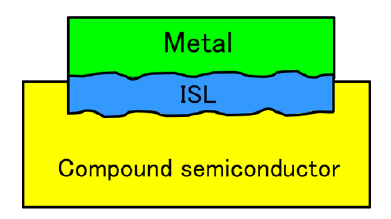
where φB, NB, and ρ0 are the Schottky Barrier Height (SBH), the dopant concentration close to the M/S interface and the preexponential factor, respectively. It is found from equation (1) that either a small φB or a large NB is required to achieve a low ρc value. The reduction of the ρc value is achieved by the ISLs formed at the M/S interface, which plays two major roles. One is the ISL containing dense carrier or donor/acceptor dopants, and the other is the ISL which reduces the φB value. Figure 1 shows a crosssectional view of the Ohmic contact material with the ISL containing high density carriers or donor/acceptor dopants (named by dense dopant ISL) and decreasing the φB at the M/S interface (named by low barrier ISL) where the heterojunction structure is formed by the low SBH and the small band discontinuity at the interface with the semiconductor. Various fabrication methods have been used to form the ISL shown in Figure 1. Specifically, the method here focuses on the metallurgy reaction to fabricate the interface structure by depositing and annealing multidimensional elements (not only metals) on semiconductors. The Ohmic contact fabricated in this way is referred to as a “Metallurgy Ohmic Contact (MOC)” material. This method is most suitable for practical device applications because once the fabrication process is established, it is very reproducible, mass production is possible, and contact materials can be fabricated inexpensively. AuNiGe is a typical example of MOC for n-GaAs which has been successfully used to form the ISL shown in Figure 1, which was first demonstrated in 1967 as an Ohmic contact for Gunn diodes [3].
Figure 1:Schematic drawing of a cross-sectional view for a metal/compound semiconductor interface with Intermediate Semiconductor Layer (ISL) [2].

The ISLs were formed because of the metallurgical reaction between GaAs and AuNiGe by annealing at 400 °C or higher from the structure composed of eutectic AuGe and Ni layers. The Ge-doped n+-GaAs ISL or n+-Ge ISL is thought to be produced [4]. NiInW, the MOC material developed by Murakami and Price in 1987 for GaAs integrated circuits, is a thermally stable Ohmic contact material formed from InxGa1-xAs as low barrier ISL [5]. In fact, the existence of InxGa1-xAs layer at the interface, which was predicted from the phase diagram analysis based on the metallurgical reaction with NiIn/GaAs, was confirmed by electron microscopy, and the low ρc was realized [6]. The issue for developing low-resistance MOC for p-GaN is that it is difficult to find effective elements to form the dense dopant and low barrier ISLs in Figure 1, which have been successfully achieved with GaAs to date. The SBH at the metal/p- GaN interface is reported to be as large as 2eV, and the ionization energy of the only acceptor element, Mg, is reported to be as large as over 200meV [2]. The highest hole concentration reported so far is about 1E18cm-3, and the maximum acceptor concentration is limited to 1E20cm-3. ρc ≈1E-5 Ω-cm2 is predicted from the theoretical calculation to require φB values below 0.3eV even at NB=5E19cm-3 for fabricating MOC materials [2]. The p-InxGa1-xN layer is a candidate for low barrier ISL at the metal/p-GaN interface and is expected to lower the SBH. Preliminary experiments have shown that it is difficult to form the InxGa1-xN solid solution layer after annealing the In layer deposited on p-GaN at high temperature. The major reason why the InxGa1-xN layer cannot be formed from In/GaN is that the phase diagram analysis predicted the miscibility InxGa1-xN alloy up to around 1300 °C [7]. Therefore, the possibility of InxGa1-xN layer formation by acceleration of metallurgical reaction under high pressure and high temperatures above 1100°C should be explored in the future. Annealing and in-diffusion process of the Mg layer on p-GaN at elevated temperature is expected to be a method to fabricate the dense dopant ISL. Recently, the ρc value of NiAu contact to annealed Mg layer on p-GaN was reported by Lu to be 1E-5 Ω-cm2 at p-GaN epilayer with Mg concentration of 1E19cm-3 [8].
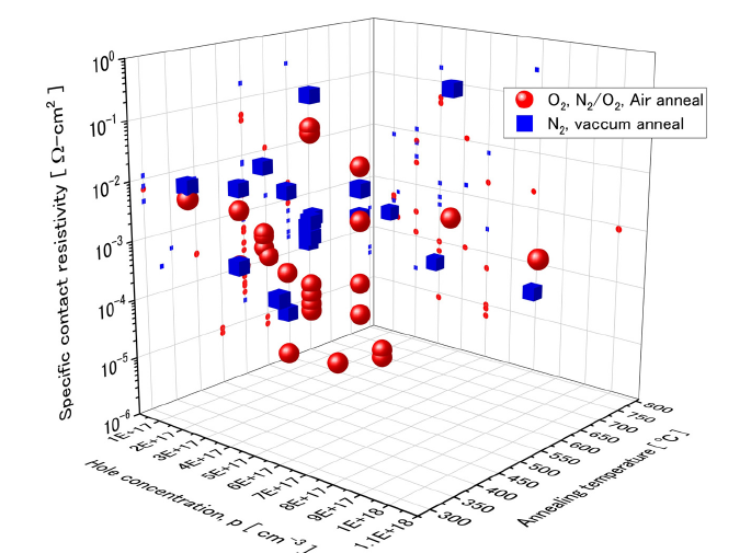
They proposed that MgGaN compound formation and heavy doping of Mg by in-diffusion which provided the low barrier and dense dopant ISLs formation [8]. As a specific phenomenon, Ho [9] and Koide [10] reported in 1999 that the ρc value of NiAu contact was reduced to 1E-5~1E-4 Ω-cm2 by annealing at 400 to 600°C in a N2?/O2 mixture or air ambient. Subsequent numerous reports have shown that the most effective MOC materials are stacked contact materials combining metals with large work functions and annealing in an ambient containing oxygen. Figure 2 shows the relationship between the ρc values, hole concentrations, and annealing temperatures for the MOC materials reported so far by oxygen annealing [11]. The mechanism of the decrease in contact resistivity is still unknown, and a variety of models such as NiO behaving as the low φB ISLs [9], the removal of hydrogen in p-GaN by O2 annealing [10], and the φB reduction to around 0.7eV [10,11]. Recently, it was reported by Mizushima [12] that the oxygen annealing reduced the SBH by about 0.1 eV based on synchrotron radiation x-ray photoelectron spectroscopy and microstructure observation. Similarly, the existence of epitaxial single-crystal phase Ga oxides with three to four molecular layers as natural oxide layer on the GaN surface has been reported [13]. It is essential to understand the formation mechanism of low barrier and dense dopant ISLs by investigating the Ga oxide and Mg-related compound formation and the defects related with the Mg dopant in the p-GaN close to the interface. On the other hand, at present InSnO (ITO)-based contacts [14] for p-GaN is known to be the standard MOC materials for LEDs and LDs since this MOC provides the low ρc value and transparent for visible right emission. The role of the oxygen on the metallurgical reaction between ITO and p-GaN is key to understand the mechanism of the ρc reduction.
Figure 2:Relationship between c values, hole concentrations, and annealing temperatures for the MOC materials reported so far by annealing in oxygen mixture and air ambient, where literature data listed in [11] are used.

Conclusion
We reviewed the guideline of low-resistance MOC materials developed for n-GaAs compound semiconductors. For n-GaAs, Ge in the AuNiGe contact and In in the NiInW contact played a key role in forming the ISLs. For p-GaN, In was the candidate element to form ISL with low φB p-type ISL, but the method to form ISL metallurgically has not been discovered yet. On the other hand, the thermal annealing in oxygen ambient and the metal/InSnO contact have been found to be effective in reducing the contact resistivity. The oxygen plays an essential role in the metallurgical reaction, but its materials science guideline remains unresolved. It is important to elucidate the mechanism and to continue to search the MOC materials with low barrier and dense dopant ISLs.
References
- Koide Y (2021) Isamu Akasaki in memoriam. Nature Photonics 15(8): 551-552.
- Murakami M, Koide Y (1998) Ohmic contacts for compound semiconductors. Crit Rev in Solid State and Mat Sci 23(1): 1-60.
- Braslau N, Gunn JB, Staples JL (1967) Metal-semiconductor contacts for GaAs bulk effect devices. Solid-State Electron 10(5): 381-383.
- Heiblum M, Nathan MI, Chang CA (1982) Characteristics of AuGeNi ohmic contacts to GaAs. Solid-State Electron 25(3): 185-195.
- Murakami M, Price WH (1987) Thermally stable, low-resistance NiInW ohmic contacts to n-type GaAs. Appl Phys Lett 51: 664-667.
- Kim HJ, Murakami M, Price WH, Norcott M (1990) Thermally stable ohmic contacts to n-type GaAs. VI. InW contact metal. J Appl Phys 67: 4183-4189.
- Adhikari J, Kofke DA (2004) Molecular simulation study of miscibility in InxGa1-xN ternary alloys. J Appl Phys 95(8): 4500-4502.
- Lu S, Deki M, Wang J, Ohnishi K, Ando Y, et al. (2021) Ohmic contact on low-doping-density p-type GaN with nitrogen-annealed Mg. Appl Phys Lett 119, 242104-1-7.
- Ho JK, Jong CS, Chiu CC, Huang CN, Chen CY, et al. (1999) Low-resistance ohmic contacts to p-type GaN. Appl Phys Lett 74(9): 1275-1277.
- Koide Y, Maeda T, Kawakami T, Fujita S, Umehara T, et al. (1999) Effects of annealing in an oxygen ambient on electrical properties of Ohmic contacts to p-Type GaN. J Electronic Mater 28: 341-345.
- Grecoa G, Iucolanob F, Roccafortea F (2016) Ohmic contacts to gallium nitride materials. Appl Surf Sci 383: 324-345.
- Mizushima M, Arai R, Inaba Y, Yamashita S, Yamaguchi Y, et al. (2021) Impact of oxygen on band structure at the Ni/GaN interface revealed by hard X-ray photoelectron spectroscopy. Appl Phys Lett 118: 121603.
- Dycus JH, Mirrielees JK, Grimley ED, Kirste R, Mita S, et al. (2018) Structure of ultrathin native oxides on III−nitride surfaces. ACS Appl Mater Interfaces 10(13):10607-10611.
- Margalith T, Buchinsky O, Cohen DA, Abare AC, Hansen M, et al. (1999) Indium tin oxide contacts to gallium nitride optoelectronic devices. Appl Phys Lett 74(26): 3930-3932.
© 2023 Yasuo Koide. This is an open access article distributed under the terms of the Creative Commons Attribution License , which permits unrestricted use, distribution, and build upon your work non-commercially.
 a Creative Commons Attribution 4.0 International License. Based on a work at www.crimsonpublishers.com.
Best viewed in


.jpg)


 Editorial Board Registrations
 Submit your Article
 Refer a Friend
 Advertise With Us
.jpg)


.jpg)


.bmp)
.jpg)
.png)
.jpg)


.jpg)


.png)

.png)


.png)


