
- About Us
- Information
-

The Author ensures that the research has been conducted responsibly and ethically with adherence to all relevant regulations. read more..
- For Authors
- For Reviewer
- Manuscript Guidelines
- Membership
- Publication Ethics
-
- Journals
- Reprints
- e-Books
- Videos
- Policies
- Contact Us
 COVID-19
- Submissions


Full Text
COJ Reviews & Research
On the design of Current Controllers for Three Phase Voltage PWM Converters
Rodrigo Guzman Iturra*
Electrical Machines and Power Electronics Laboratory, Germany
*Corresponding author: Rodrigo Guzman Iturra, Electrical Machines and Power Electronics Laboratory, Soest, NRW, Germany
Submission: January 22, 2020; Published: April 18, 2022

ISSN 2639-0590Volum3 Issue5
Introduction
There is large variety of applications that rely on DC/AC converters such as ac motor drives, STATCOMs, active power filters, uninterruptible power supplies and photovoltaic systems [1]. In many of these applications, the three phase currents that are generated by the DC/AC converter follow a reference provided by an outer loop. The current references are generated by speed controllers in the case of ac motor drives, a reactive power controller or grid voltage regulators in the case of STATCOMs and in case of photovoltaic systems they follow a reference generated based on the amount of active power that needs to be injected into the grid. Most of the DC/AC converters are based on a Voltage Source Inverter (VSI) and in order to achieve a good performance, the VSI is commanded by a current controller to track as accurate as possible the three phase currents reference. Pulse With Modulation (PWM) and Space Vector Modulation (SVM) are two techniques used in VSIs to generate the time average output voltage demanded by the current controller. By using the average model of the VSI, controlled either by PWM or by SVM, we can use feedback linear control for the analysis and design of the current controller. The main goal of this short document is to illustrate an analytical formula that in my opinion is the optimal gain for a proportional current controller based on the values of the coupling inductivity, the DC Bus voltage and the switching frequency of a three phase PWM converter.
System Modelling
Figure 1 shows the structure of the DC/AC converter based on a VSI, which represents the power electronics part. Holmes et al. [2] have shown in that each phase can be controlled independently if the three-phase system is balanced. Therefore, considering each phase independently as an individual half-bridge, the dynamics of the AC current for the three phases can be described by [3]:
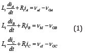
Where 𝑉Gx are the voltage of the grid and 𝑉xI is the time average voltage produced by the inverter. In 𝛼 - 𝛽
coordinates the model of the three-phase converter is as follows:
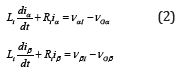
Figure 1: Voltage Source Inverter (VSI) connected to a power grid through a coupling inductor Li with an internal resistance Ri. The grid is represented by the three voltages sources vGx.

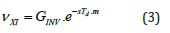
The time average voltage produced by the inverter can be controlled directly by the duty cycle (m) feed to the PWM modulator. The average model of the VSI is considered as a linear amplifier [3] with a gain 𝐺INV related with the DC bus voltage and a dead time (transport delay) introduced by the switching process [2,4].
Thus:
Where for PWM with double sample update the delay can
be approximated by  being 𝐹S the switching frequency and
 for the case of PWM.
For the controller design, many authors approximate the transport delay produced by the switching process by a first order Pade approximation [4]:
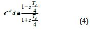
Or even they approximate the transport delay roughly by a first order system of the form [5]:
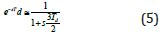
Equations (4) and (5) are a good approximation in case that the switching frequency is at least a factor of 10 times larger than the frequency of the reference signal feed to the PWM modulator. However, there is applications where this condition does not hold, for instance in high power applications when the switching frequency cannot be high due to unacceptable switching losses or in case of active power filters that compensate high order harmonics. In such cases the approximation will lead to a bad performance of the current controller or even to instabilities in the current control loop [6]. Therefore, for such applications is better to design the current controller considering the transport delay directly in the model.
Open Loop Transfer Function
By disregarding the voltage of the grid 𝑉Gx that acts just a disturbance and can be almost entirely canceled by feedforward controller as is explained in [3], the open loop transfer function for the current loop considering the transport delay and a proportional controller is as follows:
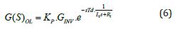
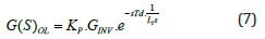
The resistance of the coupling inductivity 𝑅i that is usually smaller compared with the reactance can be neglected, it follows:
Derivation of Optimal Proportional Gain
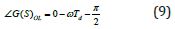
The following derivation follows the procedure described on [2], furthermore is this document the derivation is done in a stepby- step fashion and at the end a final analytical formula is achieved. The phase angle of the frequency dependent expression (7) is equal to:
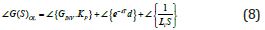
𝐾P and 𝐺INV are just gains and their contribution to the total
phase is 0 °, the coupling inductivity is always
contributing -90 ° or rad to the total phase when 𝑅i is neglected.
The dead time is introducing negative
phase in radians that is linearly proportional to the frequency
Franklin et al. [7], thus:
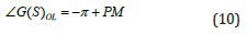
The phase of the open loop transfer function can be made function of the desired Phase Margin (PM) according to:
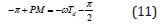
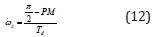
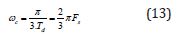
If we choose certain PM, we can use equation (10) to calculate which cross over frequency 𝜔c corresponds to the selected PM margin:
A PM of 30 ° or rad , produces a close loop with a damping
ratio of approximate 0.3 that should be adequate to track without
that much error sinusoidal references and it is judged as the lowest
adequate value for the phase margin according to Franklin et al. [7].
For a PM = 30 ° and  in (12),
it follows:
The proportional gain 𝐾P to achieve 𝜔c can be calculated by the gain expression in dB of the open loop transfer function:
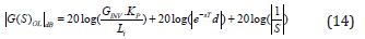
The dead time element is always contributing 0 dB to the overall gain of the system and the integrator produces -20dB per decade thus:
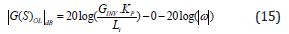
At the cross over frequency 𝜔c the gain of the open loop system is 
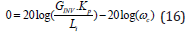
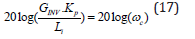
Thus:
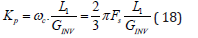
Optimal Proportional Gain for PWM - 2 Level (2L) and 3L NPC
The static gain for the case of the 2-level inverter using PWM is  therefore the optimal
proportional gain is finally:
therefore the optimal
proportional gain is finally:
According to Yazdani [3] the average model of the 3 Level NPC topology is the same as the 2 level PWM inverter topology, model that was illustrated in equation (2). It follows that the gain calculated by the expression (18) is valid for both topologies, 2L PWM and 3L NPC PWM.
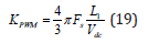
Optimal Proportional Gain for Space Vector Modulation (SVM) – 2L
Holmes [2] and Mohan [7] stated that the maximum amplitude of the output phase voltage (for a waveform measured in reference to the center point of the DC bus) for a sinusoidal reference voltage at one frequency is given by:
In case of SVM, the maximum amplitude of the output phase voltage is limited within the inner circle of the hexagon, in order to do not exceed the carried period, and it is given by [8]:
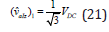
Just by inspection and comparison we can conclude that the inverter
gain in case of SVM is  and therefore the optimal
proportional gain in case of space vector modulation is given by:
and therefore the optimal
proportional gain in case of space vector modulation is given by:
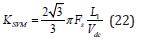
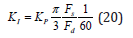
Optimal Integral Gain
If it is wanted to add an integral term with and integrator in parallel with the proportional controller, the following expression is suggested for the integral gain:
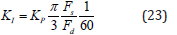
The integral gain has been calculated in such a way that the cross over frequency and the phase margin are just determined by the proportional gain in equation (18). In other words, the proportional gain calculated by (22) does not introduce any phase lag at the cross over frequency desired [9].
Conclusion
This document has shown the derivation of an analytical formula to calculate the proportional gain of a current controller for a three PWM converter. The analytical formula is easy to follow; it only depends on the parameters of the three phase PWM converter. The idea behind the formula is to guarantee always a gain that maintains the inner current loop stable with a controller that provides a fast response. Furthermore, the formula can be used on an adaptive current controller when a nonlinear coupling inductivity is used. When the last is the case, based on the current reference at certain moment and a loop-up table with the L-I characteristic of the coupling inductivity, the proportional gain can be recalculated all the time for new current references feed to the current controller.
References
- Kazmierkowski MP, Malesani L (1998) Current control techniques for three‐phase voltage‐source PWM converters: A survey. IEEE Trans Ind Electron 45(5): 691-703.
- Holmes DG, Lipo TA, McGrath BP, Kong WY (2009) Optimized design of stationary frame three phase AC current regulators. IEEE Trans Power Electron 24(11): 2417-2426.
- Yazdani A, Iravani R (2010) Voltage‐sourced converters in power systems, Oxford Press, Wiley, Hoboken, New Jersey, USA.
- Buso S, Mattavelli P (2015) Digital control in power electronics. Synthesis Lectures on Power Electronics 1: 1-229.
- Blaabjerg F (2017) Control of power electronic converters and systems. Amsterdam, Academic Press, Cambridge, Massachusetts, USA.
- Silva GJ, Bhattachaiyya SP, Datta A (2005) PID controllers for time‐delay systems. Boston, Massachusetts, USA.
- Franklin GF, Powell JD, Emami‐Naeini S (2019) Feedback control of dynamic systems. Pearson, New York, USA.
- Mohan N, Undeland TM, Robbins WP (2003) Power electronics, Converters, applications, and design. Wiley, Hoboken, New York, USA.
- Holmes DG, Lipo TA (2003) Pulse width modulation for power converters. Great Britain, John Wiley, Hoboken, New York, USA.
© 2022 Rodrigo Guzman Iturra. This is an open access article distributed under the terms of the Creative Commons Attribution License , which permits unrestricted use, distribution, and build upon your work non-commercially.
Editor In Chief


.jpg)


Signup for Newsletter

Quick Links
 Editorial Board Registrations
 Submit your Article
 Refer a Friend
 Advertise With Us
Our Recent Edition

.jpg)


Top Editors


.jpg)


.bmp)
.jpg)
.png)
.jpg)


.jpg)


.png)

.png)


.png)


Financial Support

Sponsors

Latest e-Books

Latest Video

 a Creative Commons Attribution 4.0 International License. Based on a work at www.crimsonpublishers.com.
Best viewed in
a Creative Commons Attribution 4.0 International License. Based on a work at www.crimsonpublishers.com.
Best viewed in