
- About Us
- Information
-

The Author ensures that the research has been conducted responsibly and ethically with adherence to all relevant regulations. read more..
- For Authors
- For Reviewer
- Manuscript Guidelines
- Membership
- Publication Ethics
-
- Journals
- Reprints
- e-Books
- Videos
- Policies
- Contact Us
 COVID-19
- Submissions


Full Text
COJ Electronics & Communications
An Overview and Outlook on Silicon-On- Insulator Based CMOS and FinFET Technology
Aamar Shabir and Muhammad S Ullah*
Florida Polytechnic University, Florida, USA
*Corresponding author:Muhammad S Ullah, Florida Polytechnic University, Florida, USA
Submission: January 17, 2024;Published: January 31, 2024

ISSN 2640-9739Volume3 Issue1
Abstract
Silicon-On-Insulator (SOI), considered the technology of the ‘future’ for a long time, is currently regarded as the most attractive candidate for low voltage circuits. Considerable progress in developing techniques for growing single-crystal SOI substrates suitable for fabricating high-performance devices has been foreseen. In this last decade, SOI MOSFET technology has shown its potential for high-frequency commercial applications, including K/Metal gate, Large-Scale Integration (VLSI), memory, analog and digital integrated circuits, and mixed signals. The SOI technology enables scaling to substrate 22nm gate thickness, superior leakage current control, and elimination of bipolar latch up. Moreover, transition to the SOI is essential to meet the performance and scaling. This paper reviews the SOI technology with MOSFET devices and the various technological approaches, interests, limitations and future of SOI-MOS (Metal Oxide Semiconductor) and FinFET technology.
Keywords:SOI technology; Moore’s law; MOSFET scaling; CMOS technology; FinFET technology; High-K/ Metal
Introduction
Electronic circuits have evolved to high-performance ultra-large-scaled integrated circuits made of silicon CMOS transistors and have been key elements for modern human society. Today’s high technologies, such as the internet, cellular phones, game machines, along entertainment robots, can never be realized without recent tremendous progress in integrated circuits. Traditional scaling encountered many limitations in the industry by using substrate engineering [1]. As a result, device architecture has become intimately connected, a connection that is intensifying as the IC industry progresses to nanoscale technology nodes with smaller dimensions. In 1963, Frank Wanlass and C.T Sah Fairchild unveiled the first logic gate in which p-n Chanel transistors were used in a complementary symmetric circuit configuration called CMOS today, which draws almost zero static power [2]. The first microprocessor was announced by Intel in 1971 [3]. In the 80’s, power dissipation became a serious issue due to the more static power consumption of the NMOS as compared to CMOS. Due to features like low power, reliable performance, and high speed, CMOS technology was implemented and replaced. NMOS and bipolar technology are nearly all digital applications [4]. Over the next years, CMOS scaling and improvement have enhanced the devices’ circuit speeds, chip size, and performance to cost ratios.
Industry transition to SOI technology started in the mid-90s. SOI technology reduces parasitic leakage, capacitance and power consumption. It makes it possible to increase the derived current, thus improving device performance. SOI consists of devices on silicon thin film placed on the insulating film. SOI has allowed the CMOS technology to develop solutions for high-performance logic [3]. SOI refers to the use of a three-layered substrate in place of a conventional bulk silicon substrate [5]. On top of an insulator like silicon dioxide (SiO2), sometimes known as a buried oxide layer, a thin silicon layer is deposited. This layer is positioned over the substrates and separates the body from the substrate [3,4]. Figure 1 illustrates an outline sketch of the SOI-MOS device. This paper discusses a comprehensive study of SOI-CMOS technology, and Section 1 introduces SOI-CMOS technology. Section 2 explains the CMOS study and SOI-based CMOS devices and scaling motivation is explained in Section 3. The new innovative de-vice structure and its types are explained in Section 4. Fabrication of SOI in CMOS IV characteristics of SOI CMOS devices are followed by Section 5 and Section 6. expresses IV characteristics of SOI CMOS devices advantages of SOI over bulk CMOS technology and Section 7. will summarize all aspects of the SOI-CMOS technology future endeavors. Figure 1 shows the SOI-CMOS device, which shows the buried oxide layer isolating the gate oxide from the silicon substrate [6]. After the thin silicon layer is created, transistors are constructed onto it [2,3].
Figure 1:An outline sketch of SOI-MOS device [2].

Structure of CMOS
The increasing performance and complexity brought forth by MOS scaling have fueled various applications. New information processing devices and architectures have been widely found in academia and industry as dimensional scaling CMOS finally con-fronts primary constraints [7]. For a CMOS transistor, metals are used for the gate, SiO2 (Oxide) is used as the insulator and a semiconducting material serves as the substrate [8]. The transistor’s electric field via the gate oxide activates and deactivates the gate. The conductor may identify two distinct MOS architecture types they use: (I) n-channel MOS and (II) p-channel MOS [7,8]. In this article, we will focus on the NMOS transistor because of the complimentary nature of the two varieties.
Working principle of CMOS
The drain, source, gate and substrate comprise the four terminals of a Metal-Oxide-Semiconductor (MOS) transistor [7].
The NMOS structure is shown in Figure 2. P-type silicon is the base material for the NMOS transistor (body). An insulator separates the top of the device, where a low-resistance electrode has been constructed [9]. The n- and p-type doped polysilicon utilized as gate material is the norm [10]. Insulation is provided by silicon dioxide (SiO2 or oxide). The drain and source are created by doping both sides of the substrate with donor impurities [9,10]. These locations, shown by n+ in Figure 2, are highly doped with donor impurities [8-10]. The low resistivity of these places directly affects the extensive doping [11]. Suppose the potentials of two adjacent n+ areas are skewed differently. In that case, the n+ region with the lower potential will serve as a source, while the other will function as a drain [12]. It may switch the drain and source connections depending on the applied voltage. The width-W and the length-L of the channel, the area between the source and the drain, are crucial in determining the MOS transistor’s properties [13]. Initially, aluminum was used as the gate material [7]. As MOS manufacture began with doping source and drain regions [7,8], a shift from aluminum to polysilicon occurred for various reasons. The gate oxide area that would become the aluminum metal gate was subsequently defined using a gate mask [8]. The main problem with this fabrication is that the gate mask is not perfectly aligned. In Figure 3, it can be seen how this parasitic overlap between the Cgd and Cgs is created. An even more difficult feedback capacitance than Cgs is Cgd. Miller capacitance slows down the transistor’s switching and speed [9]. This CMOS problem is addressed using the Self Aligned Gate Process [7]. Using ion implantation to form the Gate area [9] we create the source and drain regions. Figure 3 [11] shows how the capacitances may be reduced by aligning the gate concerning the source and drain using the gate oxide as a mask during doping. Figure 4. depicts the widespread use and high demand for CMOS technology.
Figure 2:The structure of NMOS [6].

Figure 1:(a) Conventional MOSFET with Parasitic capacitance.
(b) First step to form the gate insulator.
(c) Formation of the precise gate for the desired distance of source and gate.
(d) Final self-aligned device with faster operational speed and reduced parasit-ic capacitance.

Figure 4:Demand for CMOS technology [ITRS Data].

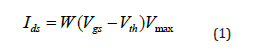
In the MOS transistor, the gate voltage decides whether current will flow between the drain and the gate. Figure 5 [13] illustrates that the gate contains positive charges. When Vgs is applied, minority carriers of a p-type substrate termed holes are repelled by positive controls [14]. These holes leave behind acceptor ions with a negative charge, which produces a depletion area [13,14]. If the value of Vgs is raised, the surface will eventually attract electrons [15]. Furthermore, abundant electrons are drawn to the surface [16]. This occurrence is known as inversion. During the inversion process, the surface of a p-type body typically contains many holes, whereas newer surfaces have many electrons [14-17]. The basic model is shown in equations 1 and 2. It is used to draw Figure 5 for different technologies portly in R language.
Figure 5:The I-V Characteristics of NMOS (a) linear scale, (b) logarithmic scale, (c) Id-Vds Characteristics.

Both the source and drain body are maintained in reverse bias. In Figure 6, the bias from the source to the body is zero [15].
Figure 6:I-V characteristics of PMOS in terms of (a) Id-Vgs, and (b) Id-Vgs.

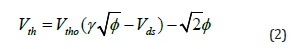
In equation 1 and 2: Ids Is drain to source current ∅ is the surface potential, W is the channel width, the gate to source voltage Vgs, Vth is the threshold voltage, Vmax is the device’s maximum voltage. As source to body potential is less positive than drain to body potential, the reverse bias across drain to body is greater, resulting in a deeper depletion under the drain area than under the source region [16]. When a voltage is supplied between the drain and source, electrons flow from the source via the conducting channel and are drained by the drain. Id (Positive current) flows from drain to source [15,17]. The IV characteristics of the NMOS are shown in Graph 2 when its Vds is 1.20V and its tox is 2nm. For various technologies, the gate length was 4 to 20nm, and the width was 4 to 20nm, the electron mobility was 1000 cm2/(Vs), and the thickness was 2,4,6,8nm. Vsb=0, ND=5 temperature= 300K, Substrate doping: NA=1015cm3. The value of drain current changes as technology shrinks and the performance of PMOS and NMOS devices improves with reduced power consumption. According to ITRS’s 2022 report [15], the gate length of the transistor has shrunk to less than 10nm. The IV characteristics of the NMOS, which operates in a linear mode of operation are depicted in Figure 5(a&b). The illustrative nature of the curve is evident in (a) as the size of the technology decreases, the gate oxide value decreases, the value of Id decreases and the Ion decreases, resulting in improved device performance. Figure 5(c) demonstrates that when the gate thickness grows, both the Id and the latency of the device increase. In Figure 6 (a&b), the value of Ids grows linearly with an increase in the drain to source voltage. (Vds) and Vgs (gate-to-source voltage). However, in the saturation region, the value of Ids remains constant and is independent of Vds. The value of Vds, derived by equation 3, is used. Results are depicted in Figures 6 (a&b).
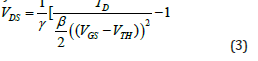
Drain to source voltage VDS, VGS gate to source voltage, VTH Threshold voltage, β is the transconductance of the channel and γ is the channel length modulation parameter.
Scaling motivation and its impacts on the CMOS devices
Growing applications have increased the need for battery powered gadgets [16]. The disadvantage of utilizing the battery is its limited power, which is not improved by 30% every five years. Moore’s law was proposed by Gorden E. Moore in 1965 about the number of transistors. By decreasing channel length, switching activities are accelerated [16]. Regarding capacitance, the power consumption decreases, while scaling a transistor result in the development of new technologies. The “channel edge effects” are insignificant for long channel devices, and the electric field lines are perpendicular to the channel surface [11-17]. The longitudinal electric field is regulated by drain-source voltage and is perpendicular to the current flow. If the channel length is less than the source and drain depletion widths, the device is said to have a short channel [18-21]. These are the consequences of short channels:
Carrier velocity saturation and current: Mobility degradation: The drift velocity of electrons in a channel is proportional to the electric field gradient [16]. At large electric fields, these drift velocities tend to saturate; this phenomenon is known as velocity saturation [18]. Because of greater vertical electric fields, the channel’s Carriers disperse off the oxide interface [18]. The oxide interface decreases carrier mobility and drains current [17,18].
Drain-Induced Barrier Lowering (DIBL): A larger drain voltage reduces the threshold voltage (Vt) [19]. Insufficient gate barrier leads to possible flow-resisting obstacles. Increased gate potential reduces the potential Barrier [20]. This potential Barrier is regulated by both Vgs and V ds in short-channel devices. The drain voltage is related to the expanding and growing depletion area. Drain-induced Barrier lowering (DIBL) refers to the drain lowering the channel barrier and decreasing the threshold voltage [19-21].
Punch through: Punch-through is an extreme instance of Barrier lowering in which, as the drain rises, the depletion zone enlarges and touches [20]. It is referred to as punch-through. Therefore, the gate voltage no longer governs the drain current [19,20]. The key cause for punch-through in the transistors is that the current transport happens deeper in bulk and far away from the gate. Therefore, the subthreshold leakage current is raised, increasing energy consumption. The punch-through current quantity is mostly based on the applied drain voltage and the source/drain junction thicknesses. A way to lessen the punchthrough effect is to raise the doping level in the transistor body (bulk). As a result, there will be less of a drain and source depletion zone and no parasitic current route will be created. Furthermore, as the subthreshold swing grows with increased transistor body doping, this approach is not suggested for minimizing drain-source leakage. Additionally, spatially controlled dopant implantations such as (a) halo or pocket implantations and (b) delta doping may be used to prevent punch-through.
Hot carrier effect: For smaller geometric devices, the electric field increases particularly near the drain [20]. These are known as warm drains. This results in the release of high-energy electrons, which may trigger impact ionization and form additional electronhole pairs [20]. Hot carrier effects are induced or exacerbated by decreasing the device’s size but not the operating voltage. As a result, the issues caused by hot carrier injection are a significant roadblock on the path to increased circuit density. Recent research has proven that hot carrier effects may still be detected even at low drain voltages (such as 1.8 V).
Therefore, the greatest way to overcome hot carrier concerns is the optimal design of devices to reduce, if not avoid, hot carrier impacts. The placement of self-aligned n-regions between the channel and the n-n-junctions to form an offset gate, graded drain junctions, and the usage of buried p+ channels are all common design strategies for mitigating hot carrier effects. Because charge de-trapping is slowed at low temperatures, hot carrier phenomena may proceed more quickly under these conditions. The following is a simplified model of the acceleration caused by hot carrier effects:
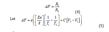
where:
The mechanism’s acceleration factor or AF;
In the first case, R1=The rate at which hot carrier effects occur
under the first set of parameters (V1 and T1);
R2=Rate of hot carrier effects at temperature and voltage of V2
and T2;
Where:
R1 and R2’s T1 and T2 are the correspondingly applied
temperatures in degrees Kelvin.
Energy dissipation potential (E)=-0.2 to -0.06 eV;
Energy dissipation potential (Ea)=-0.2 to -0.06 eV.
Short channel effect: The short channel effect can be reduced by decreasing the depletion zone’s width [21]. A small channel restricts the length of the gate. It is accomplished by raising the channel doping concentration, the gate capacitance, or both [20,21]. It may be shown via Equation 1.
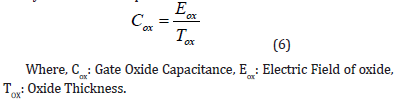
An inversion layer, formed and maintained at the channel’s surface, is crucial to the flow of current through it. Without a sufficient gate bias voltage to induce a surface flip, a potential barrier blocks the passage of channel carriers (electrons) (VGSVT0). Carriers are free to move in response to the channel electric field when this potential Barrier is decreased by increasing the gate voltage. The difference between the Gate-to-Source (VGS) and Drain-to-Source (VDS) voltages in small-geometry MOSFETs sets the potential Barrier. As the drain voltage rises, the channel potential Barrier falls; this effect is known as “Drain-Induced Barrier Lowering” (DIBL). In a MOSFET, the threshold voltage is the voltage between the device’s source and drain, although electrons may flow from the source to the drain if the potential Barrier between the gate and source is decreased. The sub-threshold current is the current in the channel at voltages below the threshold value calculated through equations (4), (5) and (6), respectively.
New innovative device structure: When the channel length is shortened, the gate has less influence on the channel in a conventional MOS design [22]. When this happens, there is an increase in drain-to-source leakage below the detection threshold [23]. The gate of a typical MOS device cannot alter the leakage route [22,23]. Different MOS are used to enhance this. As a result, a novel MOS structure called SOI is used to optimize the capacitance between the gate and the channel while simultaneously decreasing the drain’s capacitance to the channel [24].
SOI-CMOS device structure: In substitute of traditional bulk silicon wafers, Silicon on Insulator (SOI) uses a three-layer substrate consisting of a Silicon Dioxide (SiO2) insulator termed buried oxide, a silicon layer, and a silicon epitaxial layer [21]. As a result, the body is protected from the substrate by this layer [25]. This thin silicon layer is used to construct the transistors, which decreases parasitic capacitance and boosts the device’s performance [21-23]. The insulating layer most suited for a certain task must be selected accordingly. Figure 1 depicts the basic layout of an SOI-CMOS device.
There is a significant need for SOI technology because it will allow for the extension of Moor’s Law over 28nm by improving upon the standard planar core CMOS technology and (i) It will allow for higher performance. (ii) It will reduce the interaction between the devices and the substrate, which results in parasitic capacitance between the dispersed source and drain of the device, and (iii) account for increased difficulties in scaling traditional bulk CMOS. (iv) To avoid latch-up, which arises when parasitic PNP and NPN Bipolar Junction Transistors (BJT) are formed between the Vdd and Vss rails in a bulk CMOS [26]. In addition, the positive feedback from the supply rail to the ground forms a virtual short-circuit via these BJTs. As the transistor size decreases, the gate length decreases, resulting in less control over the channel and worse device performance (Figure 7). To counteract this, SOI allows more control over the channel via body biasing [23,26]. Subthreshold and diode leakage currents also contribute less to the overall leakage power [22]. We need SOI because it simplifies CMOS production while maintaining high performance, low cost, and great efficiency in energy and heat dissipation [21-26].
Figure 7:NMOS Transistor in Inversion Region [13].

Types of SOI Devices
Two types of SOI devices exist: Partially Depletion Silicon on Insulation (PD-SOI) and Fully Depleted Silicon on Insulation (FDSOI). Most commercial integrated circuits use partially depleted devices; their construction is described below.
Partially depleted
Figure 8(a) depicts a PD SOI MOSFET, which exhibits a modified changing threshold point depending on the history of the circuit because of the top silicon layer being thicker and the holes being pushed towards the buried oxide layer, creating a region called the floating body, which can store charge. [27]. If the depth of the body is less than the inversion area, the body will float in the channel [28]. The channel is doped, and the insulating buried oxide layer is thicker. Without such a charge, the substantially depleted device might collect in the body and change its characteristics [29]. We do not need wells or trenches. Therefore, the technology is much easier. The top silicon layer is 50-90nm thick and is employed in analog circuits and doped channels [29,30]. The insulating BOX layer has a thickness of 100-200nm.
Figure 8:(a) Partially depleted SOI -CMOS device [21]. (b) Fully depleted SOI -CMOS device [21].

Issues with PD-SOI: The Role of Past Events Unlike in bulk CMOS, the PD-SOI does not tie the body of the NMOS or PMOS Transistors to Vss for NMOS or Vdd for PMOS [31]. The threshold voltage varies from person to person due to variances in body voltages. Because of this, there may be discrepancies in timing between two identical devices [30-35]. The body Voltage of the switching transistors will change from their steady-state position while the SOI circuit is toggled on and off. The term for this is the “history effect.” The previous source, gate, and drain voltages determine the precise voltage. Switching speed and parasitic capacitance in a circuit are affected by the body voltage due to the channel’s proximity to the body [36-39]. To reduce the impact of short-channel effects, PD SOI MOSFETs need to have highly doped channels [31-37].
Fully depleted SOI devices
Two significant modifications to bulk CMOS technology define FD-SOI (Figure 8b) as a planar process technology. The silicon substrate has an insulating layer termed the buried oxide deposited on top of it first. Later, the PMOS and NMOS devices are implemented by placing a very thin silicon film on top of the insulating layer [40]. Due to the very thin silicon layer underneath the gate, the channel does not need to be doped to eliminate mobile charge carriers [39,41]. Because the depletion zone extends the whole-body length when the channel is narrow and weakly doped, the floating body region disappears in this case [42]. Ultra-thin body of the device and buried oxide Fully Depleted SOI [43] describe the confluence of these two breakthroughs. The insulating buried oxide layer reduces parasitic capacitance between the source, drain, and substrate. The leakage current of the channel to the substrate is much reduced because the insulator layer effectively encloses the electron flow from the source to the drain, improving power management and faster performance at lower voltage. The ultra-thin buried oxide improves the efficiency of body biasing in restricting the transistor channel [44]. The top silicon layer is typically 5-20nm thick for lowpower applications or undoped channels, while the insulating BOX layer is between 5 and 50nm thick [41-47].
Body biasing
To improve transistor performance, a substrate voltage may be applied. This technique is known as body or back biasing facilities, resulting in quicker transistor switching. Due to leaking current and decreased transistor shape, bulk COMS body biasing is very restricted [47,48]. Due to the ultrathin insulator layer in FD-SOI, the body biasing formed a buried gate underneath the channel, causing FD-SOI to behave similarly to a vertically double-gate transistor [48]. Different voltages may be given to the top and buried gates, thus altering the transistor’s properties. Depending on the voltages supplied to the top buried gates, FD-SOI may operate in either a high-performance or low-power mode [43]. The buried gate eliminates leaking in the substrate and permits a much higher voltage on the body, improving performance. FD-SOI demonstrates enhanced power efficiency, less heat dissipation, and longer battery life for portable devices. It may run at a lower voltage than bulk CMOS while providing superior performance. It renders the FD-SOI chip cooler and more energy-efficient. Dopant use is drastically reduced in FD-SOI, hence minimizing process fluctuations. It permits the transistor to run quicker at a given voltage since less process flexibility margin is permitted. FD-SOI is a planar technique that reuses most bulk CMOS processing stages [44- 49]. The manufacturing process in FD-SOI is simpler, resulting in decreased production costs and cycle time [50-55]. Due to the lack of channel doping and well implantation in FD-SOI, analog circuits may be made smaller and simpler, with improved performance at less operating power [49-55]. Numerous techniques have been employed in the field of SOI materials, including (1) Homoepitaxial techniques, (2) heteroepitaxial techniques, (3) Recrystallization techniques, (3) SIMOX (Separation by Implanted Oxygen), (4) FIPOS (Full isolation by oxidized porous silicon), (5) Unibond, (6) Eltran and Wafer Bonding [51].
Figure 9:Shows CMOS fabrication by SOI technology (a) SOI Structure, (b) Island Formation, (c) Polysilicon gate, (d) P+ drain and source, (e) N+ drain and source, (f) Metallization.

The subsequent steps for the fabrication of CMOS SOI are like Bulk Technology. The steps used in the fabrication of SOI are shown in Figure 9. Step 1 is used to form just a simple SOI structure (Figure 9(a)) of the device and step 2 involves island formation on the top of the general structure (Figure 9(b)). Step three is very important because it has polysilicon gate formation, which is used in forming N+ and P+ drain and source, as illustrated in Figures 9(c&d). A final device having PMOS and NMOS is shown in Figure 9(e&f). Figure 10 the results for the two technologies’ I-V characteristics for SOI and Bulk-CMOS. The value of Id is improved with the SOI fabrication to the CMOS technology by changing the values of the gate oxide thickness for different technology nodes. As technology is shrinking, the value of the Id is improving, and the power consumption is becoming more and more efficient, as shown in Figure 10(a).
Figure 10:Comparison between the SOI device and Bulk-CMOS device (a) Id-VDS characteristics, and (b) Combined result for the PMOS and NMOS.

I-V characteristics of SOI -CMOS devices
Channel and gate thickness govern the Id. Below the threshold value, the current is limited and diffusion currents dominate. In the PN junction of SOI-CMOS, current depends exponentially on the applied voltage. SOI-based devices overcome this problem of the injection of the electrons into the Chanel and we can see the improved Id value in the graph 4(a) depicts different values of Vgs for MOS bulk and SOI-based CMOS and got improved results shown in Figure 10(b). Consequently, Table 1. compares the bulk CMOS and SOI-CMOS technology. It can be observed from Table 1. that the advancement in the IC industry by introducing the SOI-CMOS devices substantially improves the performance of the devices.
Table 1:Comparison of SOI-CMOS vs. Bulk-CMOS.

Advantages of SOI over bulk CMOS technology
SOI-CMOS provides the following benefits over bulk-CMOS. The buried oxide layer provides enhanced electrostatic control of the channel, decreased parasitic junction capacitances, superior latchup immunity (BOX), Limited short channel effects as compared to bulk CMOS technology, decreased subthreshold leakage and diode leakage, increased speed and decreased power consumption. Offers a high-performance and cost-effective alternative to bulk CMOS technology, a compact transistor saves a great deal of space, increases packing density and is resistant to radiation. Reduced soft error rates, which relate to the alteration of data in the memory for space applications due to radiations, require fewer production and processing steps than bulk CMOS technology, simpler technology with no wells and trenches and reduced substrate noise because of the submerged oxide layer’s dielectric barrier function [50- 55]. The buried oxide’s poor thermal conductivity leads to selfheating. History of the impact in PD-SOI (Floating body effect). The complexity of thin body SOI wafer fabrication in FD SOI. These are some essential terms that the researchers must address [51].
Fin-FET SOI technology
Chenming Hu, a former chief technology officer of TSMC and current professor at Berkeley, created FinFET in 1999, followed by UTB-SOI (FD SOI) in 2000. Both designs are based on the basic concept of a thin body, which puts the gate capacitance closer to the whole channel. Less than or equal to 10 nm separates the skin from the body. Therefore, no escape route for water is too far from the entrance. Due to the capabilities of the gate, we can effectively manage the leakage [45]. The fundamental structure of FinFET would be a channel controlled by several sides of the channel. Figure 7(a&b) are examples of Double-Gate and Fin-FET SOI structures, respectively. The channel is horizontal in bulk MOS (sometimes called “planner MOS”). At the same time, the FinFET channel is vertical. Thus, the width of a FinFET device is determined by the channel’s (Fin) height [32]. The optimal channel width is calculated with the help of Equation 7.

Increasing the channel width, or the height of the Fin, raises the driving current of the FinFET. Constructing numerous fins in parallel and linking them together, as illustrated in Figure 10, may further boost the device’s driving current. Since the channel width of a FinFET is always a multiple of the fin height, this rules out the possibility of an arbitrary channel width. Because of this, the device’s effective width is now quantized. In planner devices, the channel width allows the user to customize the device’s driving strength [30-36]. Traditional MOS employs channel doping to mitigate SCEs and guarantee a high Vth. FinFET makes channel doping discretionary since its gate structure is wrapped around the channel and its tiny body provides greater SCEs. It suggests that FinFET is less affected by dopant-induced fluctuations. Low channel doping also improves carrier mobility inside the channel [2,3]. That means enhanced efficiency. It has been observed that a new scaling parameter, Body Thickness, has been added in both FinFET and SOI technologies [4,5]. Many benefits of FinFET technology over bulk CMOS include greater drive current for a given transistor footprint, leading to faster speed, reduced leakage, leading to lower power consumption [6] and less random dopant fluctuation, leading to improved mobility and scaling of the transistor beyond 28nm [43- 47].
Fin-FET SOI and bulk fin-FET
MOSFETs must be scaled down significantly with emerging materials to get high integration density and performance [7]. Problems with threshold voltage (Vth) reduction, Subthreshold Swing (SS) degradation, Drain-Induced Barrier Lowering (DIBL), device characteristic fluctuations with random channel dopant, leakage increase due to dielectric tunneling and band-to-band tunneling at the junction have plagued the scaling of conventional planar MOSFETs in the sub-50nm regime [57]. Several device topologies, including thin-body Silicon-on-Insulator (SOI) MOSFETs [31], double-gate MOSFETs [56], triple-gate MOSFETs [55], and fin-shaped field-effect transistors (FinFETs) [57,58], have been suggested to address these issues [59].
Figure 11:Comparison of bulk and SOI FinFET (a) Effect of Threshold voltage on Fin width, (b) Effect of subthreshold swing on Fin width [71].

FinFET provides greater current drivability, virtually optimal Subthreshold Swing (SS) and mobility improvement compared to other architectures, making it a strong con-tender for the ultimate CMOS device structure [60]. Two distinct categories of FinFETs exist: Silicon-on-Insulator (SOI) and silicon-on-insulator (bulk). Cross-sectional images of SOI FinFET and bulk FinFET are shown in Figure 11. Some benefits of bulk FinFETs over SOI FinFETs have been shown, and they maintain almost the same scaling-down properties as SOI FinFETs [61]. Bulk FinFETs have several benefits, including cheap manufacturing costs, a low defect density, the absence of a floating-body effect, a high heat transfer rate to the substrate, and a process flow that is substantially identical to that [60-65] of traditional bulk CMOS technology. SOI FinFETs has the potential to have superior speed characteristics than bulk FinFETs because they have a lower source/drain to substrate capacitance and can prevent leaking between the source and drain via the fin body below the channel fin [66].
In recent years, bulk FinFETs constructed on bulk Silicon (Si) wafers have been experimentally proven and their properties have been investigated [67-72]. Bulk FinFETs may be used in DRAM, SRAM, and flash memory devices. One may read about the use of Fin-FETs in high-speed logic in [52,73]. By analyzing the data in Table 2, SOI-FinFET provided preferable parameter values to MOSFET, SOI-CMOS, and FinFET. The subthreshold slope performance is impressive when comparing SOI-FinFET to Bulk- CMOS, SOI-FinFET and FinFET. SOI-FinFET is the lowest-value device among MOSFET, MESFET and FinFET in DIBL. It is also high in SCE. SOI-power FinFET’s consumption is less than Bulk-CMOS, SOI-CMOS, and FinFETs. Additionally, SOI-FinFET switches more quickly than others. Power dissipation and current leakage are drastically reduced over time [73].
Table 2:Comparison of SOI vs. Bulk-CMOS and FinFET.

Conclusion
The latest advancements in SOI technology are not to be underestimated. Research in SOI-CMOS and SOI-FinFET devices, which had stalled for over a decade, has been revitalized thanks to recent advancements that have led to improved device performance and shrunk the technology, resulting in new device designs and techniques. The sudden improvement in the IC industry due to SOI technology with good I-V characteristics is a good sign. Fabrication processes are becoming easier for emerging technology. However, cost reduction, performance improvement, and process refinement at a simple economic scale is the target for researchers. Therefore, SOI will remain a cutting-edge IC development and production technology.
References
- Martineau B, Mercier E, Vincent P (2007) Opportunity of CMOS FDSOI for RF power amplifier. (2nd edn), IEEE S3S, California, USA 3: 154-196.
- Weber O (2017) FDSOI vs FinFET: Differentiating device features for ultra-low power & IoT applications. IEEE International Conference on IC Design and Technology, Austin, USA, pp. 1-3.
- Lawrence B, Rubia J (2015) Review of Fin FET technology and circuit design challenges. J Eng Res Appl 5(12): 77-80.
- (2020) Official site of the company Soitec.
- Shelepin NA (2018) Features of the VLSI element base based on CMOS SOI technology with full depletion. Nano-industry, pp. 46-48.
- Dubois E, Larrieu G (2001) Low Schottky barrier source/drain for advanced MOS architecture: Device design and material considerations. ULIS’2001 Workshop 46(7): 997-1004.
- Amin AB, Shakil SM, Ullah M Sana (2022) A theoretical modeling of adaptive mixed CNT bundles for high-speed VLSI interconnect design. Crystals 12(2): 2073-4352.
- Shakil S, Ullah M (2022) Effect of NBTI on PMOS device with technology scaling. 2022 IEEE 13th Annual Ubiquitous Computing, Electronics & Mobile Communication Conference (UEMCON), New York, USA.
- Saha S (2001) Scaling considerations for high performance 25nm metal-oxide-semiconductor field-effect transistors. J Vacuum Science & Technology B: Microelectronics and Nanometer Structures 19(6): 2240-2246.
- Saha S (2001) Design considerations for 25nm MOSFET devices. Solid-State Electronics 45(10): 1851-1857.
- Bernstein K, Frank DJ, Gattiker AE, Haensch W, Ji BL, et al. (2006) High-performance CMOS variability in the 65nm regime and beyond. IBM J Research and Development 50(4-5): 433-449.
- Kuhn K, et al (2008) Managing process variation in intel's 45nm CMOS technology. Intel Technology J 12(2): 92-110.
- Thomas D, Narek R, Peter A (2018) A 45% PAE pMOS power amplifier for 28GHz applications in 45nm SOI. 2018 IEEE 61st International Midwest Symposium on Circuits and Systems (MWSCAS), Windsor, Canada, pp. 680-683.
- Asenov A, Kaya S, Davies JH (2002) Intrinsic threshold voltage fluctuations in Deca nano MOSFETs due to local oxide thickness variations. IEEE Trans Electron Devices 49(1): 112-119.
- Asenov A, Cathignol A, Cheng B, Mckenna KP, Brown AR, et al. (2008) Origin of the asymmetry in the magnitude of the statistical variability of n- and p-channel poly-Si gate bulk MOSFETs. IEEE Electron Device Letters 29(8): 913-915.
- Diaz CH, Tao HJ, Ku YC, Yen A, Young K (2001) An experimentally validated analytical model for gate Line-Edge Roughness (LER) effects on technology scaling. IEEE Electron Device Letters 22(6): 287-289.
- Stevanovic I, McAndrew CC (2009) Quadratic backward propagation of variance for nonlinear statistical circuit modeling. IEEE Trans Computer-Aided Design of Integrated Circuits and Systems 28(9): 1428-1432.
- Wakabayashi H, Yamagami S, Ikezawa N, Ogura A, Narihiro M, et al. (2003) Sub-10nm planar-bulk-CMOS devices using lateral junction control. IEDM Tech Dig, Washington DC, USA, pp.989-991.
- Stolk PA, Widdershoven FP, Klaassen DBM (1998) Modeling statistical dopant fluctuations in MOS transistors. IEEE Trans Electron Devices 45(9): 1960-1971.
- Shahidi G, Anderson C, Chappell B, Chappell T, Comfort J, et al. (1994) A room temperature 0.1μm CMOS on SOI. IEEE Trans Electron Device 41(12): 2405-2412.
- Han Xiao, Ru Huang, Jiale Liang S, Hongwei Liu (2007) The localized-SOI MOSFET as a candidate for analog/RF applications. IEEE Transactions on Electron Devices 54(8): 1978 - 1984.
- Majundar A, Ren Z, Koester SJ (2009) Undoped-body extremely thin SOI MOSFETs with back gates. IEEE Trans On Electron Devices 56(10): 2270 - 2276.
- Jhaveri R, Woo J (2006) Schottky tunneling source MOSFET design for mixed mode and analog applications. Eur Solid-State Device Res Conf (ESSDERC), Montreux, Switzerland, pp. 295-298.
- Zhu S, Yu HY, Chen JD, Whang SJ, Chen JH, et al. (2004) Low-temperature MOSFET technology with Schottky barrier source/drain, high-K gate dielectric and metal gate electrode. Solid State Electron 48(10-11): 1987-1992.
- Itoh A, Saitoh M, Asada M (2000) Very short channel metal-gate Schottky source/drain SOI-PMOSFETs and their short channel effect. 58th Annu Device Res Conf Dig, pp. 77-78.
- Colinge JP (2008) The new generation of SOI MOSFETs. Romanian Journal of Information Science and Technology 11(1): 3-15.
- Jiao Z, Salama CAT (2001) A fully depleted channel SOI nMOSFET. Electrochem Soc Proc, pp. 403-408.
- Gelsinger PP (2001) Microprocessor for the new millennium: Challenges, opportunities and new frontiers. Dig Tech 2001 IEEE International Solid-State Circuits Conference, San Francisco, USA, pp.22-23.
- Rappitsch G, et al. (2004) SPICE modeling of process variation using location depth corner models. IEEE Trans Semiconductor Manufacturing 17(2): 201-213.
- Adam AO, Higashi K, Fukushima Y (1999) Analytical threshold voltage model for ultra-thin SOI MOSFETs including short-channel and floating body effects. IEEE Trans Electron Devices 46(4): 729-737.
- Cheng B, Rao VR, Ikegami B, Woo JCS (1998) Realization of sub 100nm asymmetric channel MOSFETs with excellent short-channel performance and reliability. 28th Eur Solid-State Device Research Conf (ESSDERC), Bordeaux, France, pp. 520-523.
- Hakim N, Dunga MV, Kumar A, Rao VR, Vasi J (2001) Characterization of the Lateral Asymmetric Channel (LAC) thin film SOI MOSFET. 6th Int Conf Solid State and Integrated Circuit Technology (ICSICT), Shanghai, China, pp. 655-660.
- Hakim N, Dunga MV, Kumar A, Vasi J, Rao VR (2002) Analysis of floating body effects in thin film conventional and single pocket SOI MOSFETs using the GIDL current technique. IEEE Electron Device Lett 23(4): 209-211.
- Jhaveri R, Nagavarapu V, Woo JCS (2009) Asymmetric Schottky tunneling source SOI MOSFET design for mixed-mode applications. IEEE Trans Electron Devices 56(1): 93-99.
- Duvvury C, Amerasekera A, Joyner K, Ramaswamy S, Young S (1996) ESD design for deep submicron SOI technology. Dig Tech Papers Symp VLSI Technology, Honolulu, USA, pp. 194-195.
- Yamaguchi Y, Isibashi A, Shimizu M, Nishimura T, Tsukamoto K, et al. (1993) A high speed 0.6μ gate array on a thin SIM OX film. IEEE Trans Electron Devices 40: 179.
- Smith JC, Lien M, Veeraraghavan S (1996) An ESD protection circuit for TFSOI technology. IEEE Int SOI Conf, pp. 170-171.
- Mistry K, Grula G, Sleight J, Bair L, Stephany R, et al. (1997) A 2.0 V, 0.35m partially depleted SOI-CMOS technology. In IEDM Tech Dig, pp. 583-586.
- Lee S, Sakurai T (2000) Run-time voltage hopping for low-power real-time systems. Proc IEEE/ACM Design Automation Conf, pp. 806-809.
- Schepis DJ (1997) A 0.25m CMOS SOI technology and its application to 4Mb SRAM. In IEDM Tech Dig, pp. 587-590.
- Flautner K, Kim NS, Martin S, Blaauw D, Mudge T (2002) Drowsy caches: Simple techniques for reducing leakage power. In Proc 29th Annual Int Symp Computer Architecture, Anchorage, USA, pp. 148-157.
- Burd TD, Pering TA, Stratakos AJ, Brodersen RW (2000) A dynamic voltage scaled microprocessor system. IEEE J Solid-State Circuits 35(11): 1571-1580.
- Shabir A, Ullah M (200) Heat transfer characteristics of CNT with chirality engineering for solar cell application. In 2022 IEEE International Semiconductor Conference (CAS 2022), Brasov, Romania, pp. 159 -162.
- Shakil SM, Ullah MS (2022) Effects of NBTI on PMOS device with technology scaling. 2022 IEEE 13th Annual Ubiquitous Computing, Electronics & Mobile Communication Conference (UEMCON 2022), New York, USA, pp. 402-406.
- Shabir A, Ullah M (2022) Investigation of the emerging materials based high efficiency CdTe solar cell. Proceedings of the 7th North American International Conference on Industrial Engineering and Operations Management (IEOM 2022), Orlando, USA, pp. 2698-2706.
- Shabir A, Cao J, Fouad E, Ullah M (2022) Prospects of solar cell technology from silicon to carbon nanotube. In 2022 IEEE 9th International Conference on Sciences of Electronics, Technologies of Information and Telecommunications (SETIT 2022), Hammamet, Tunisia, pp. 385-391.
- Shakil SM, Rashid MH (2023) The potential impacts of wireless power transfer on the global economy, society and environment. In IEEE 14th Power Electronics, Drive Systems and Technology Conference (PEDSTC), Babol, Iran.
- Stolk PA, Widdershoven FP, Klaassen DBM (1998) Modeling statistical dopant fluctuations in MOS transistors. IEEE Trans Electron Devices 45(9): 1960-197.
- Shabir A, Ullah M (2022) Chirality engineering on CNTs: A new approach to boost the solar cell efficiency. Proceedings of the 7th North American International Conference on Industrial Engineering and Operations Management (IEOM 2022), Orlando, USA, pp. 1705-1706.
- Shakil SM, Ullah M (2023) Analysis of HCD effects for NMOS transistor with technology scaling. In IEEE Southeast Con 2023-Engineering the Magic. Orlando, USA.
- Cheng B (2001) Metal gates for advanced sub-80nm SOI CMOS technology. IEEE Int SOI Conf, Durango, USA, 3: 90-91.
- Huang X, Lee WC, Kuo C, Hisamoto D, Chang L, et al. (1999) Sub 50nm FinFET: PMOS. In IEDM Tech Dig, pp. 67-70.
- Yoshimi M, Terauchi M, Murakoshi A, Takahashi M, Matsuzawa K, et al. (1994) Technology trends of Sili-con-on insulator its advantages and problems to be solved. In IEDM Tech Dig, San Francisco, USA, pp. 429.
- Lederer D, Raskin JP (2008) RF performance of a commercial SOI technology transferred onto a passivated HR silicon substrate. IEEE Trans Electron Devices 55(7): 1664-1671.
- Neve C, Raskin JP (2012) RF harmonic distortion of CPW lines on HR-Si and trap-rich HR-Si substrates. IEEE Trans Electron Devices 59(4): 924-932.
- Bon O, Gonnard O, Boissonnet L, Dieudonne F, Haendlerl S, et al. (2007) RF power NLDMOS technology transfer strategy from the 130nm to the 65nm node on thin SOI. IEEE SOI Conference, Indian well, USA, pp. 2007.
- Shahidi G (2001) SOI technology for the GHz Era. IEEE International Symp, VLSI Technology, Systems and Applications, Hsinchu, Taiwan, pp. 11-14.
- Lee T, Lee S (2010) Modeling of SOI FET for RF switch applications. IEEE RFIC Symp, Anaheim, USA, pp. 479-482.
- Joshi AB, Lee S, Chen YY, Lee TY (2012) Optimized CMOS-SOI process for high-performance RF switches. IEEE SOI Conference, Napa, USA.
- Kashani MH, Molavi R, Mirabbasi S (2019) A 2.3-mW 26.3-GHz Gm-boosted differential colpitts VCO with 20% tuning range in 65-nm CMOS. IEEE TMTT 67(4): 1556-1565.
- Larie A, Kerhervé E, Martineau B, Vogt L, Belot D (2015) A 60GHz 28nm UTBB FD-SOI CMOS reconfigurable power amplifier with 21% PAE, 18.2dBm P1dB and 74mW PDC. IEEE ISSCC, San Francisco, USA.
- Kedzierski J, Ieong M, Xuan P, Bokor J, King TJ, et al. (2001) Design analysis of thin-body silicide source/drain devices. In Proc IEEE Int SOI Conf, Durango, USA, pp. 21-22.
- Wakabayashi H, Yamagami S, Ikezawa N, Ogura A, Narihiro M, et al. (2003) Sub-10nm planar-bulk-CMOS devices using lateral junction control. IEDM Tech, Washington DC, USA, pp.98 -991.
- Pravin JC, Prajoon P, Nesamania FP, Srikesh G, Kumar PS, et al. (2018) Nanoscale high-k dielectrics for junctionless nanowire transistor for drain current analysis. Journal of Electronic Materials 47(5): 2679-2686.
- Tinella C (2006) 0.13um CMOS SOI SP6T antenna switch for multistranded handsets. SiRF 58-61.
- Chen W, Pjencak J, Agam M, Janssens J, Jerome R, et al. (2021) A cost effective and highly manufacturable approach to extend a BCD 70V technology to 200V. Power Semiconductor Devices and ICs (ISPSD), 33rd International Symposium, Nagoya, Japan, pp. 287-290.
- Sanaullah M, Chowdhury MH (2015) Multilayer molybdenum disulfide (MoS2) based tunnel transistor. 2015 IEEE International Symposium on Circuits and Systems (ISCAS), Lisbon, Portugal, pp. 1929-1932.
- Sanaullah M, Chowdhury MH (2015) Subthreshold swing characteristics of multilayer MoS2 tunnel FET. 2015 IEEE 58th International Midwest Symposium on Circuits and Systems (MWSCAS), Fort Collins, CO, USA, pp. 1-4.
- Sanaullah M, Chowdhury MH (2015) Optimization of ON current in multilayer molybdenum disulfide (MoS2) based tunnel field effect transistor. 2015 IEEE 58th International Midwest Symposium on Circuits and Systems (MWSCAS), Fort Collins, USA, pp. 1-4.
- Lee JH (2009) Comparison of SOI FinFETs and bulk FinFETs.
- Ullah MS, Chowdhury MH (2017) Optimization of subthreshold swing for multilayer MoS2 tunnel transistor. 2017 IEEE 60th International Midwest Symposium on Circuits and Systems (MWSCAS), Boston, USA, pp. 981-984.
- Shabir A, Ullah M (2022) Explore the chirality engineering of carbon nanotubes for solar cell. Florida Scientist 85(2): 68.
- Shabir A, Irshad U, Shoaib M, Abeer H (2023) Design of MR damper for automobile suspension with finite element method. 8th North America Conference on Industrial Engineering and Operations Management, Houston, USA.
© 2023 Anle Mu. This is an open access article distributed under the terms of the Creative Commons Attribution License , which permits unrestricted use, distribution, and build upon your work non-commercially.
Editor In Chief


.jpg)


Signup for Newsletter

Quick Links
 Editorial Board Registrations
 Submit your Article
 Refer a Friend
 Advertise With Us
Our Recent Edition

.jpg)


Top Editors


.jpg)


.bmp)
.jpg)
.png)
.jpg)


.jpg)


.png)

.png)


.png)


Financial Support

Sponsors

Latest e-Books

Latest Video

 a Creative Commons Attribution 4.0 International License. Based on a work at www.crimsonpublishers.com.
Best viewed in
a Creative Commons Attribution 4.0 International License. Based on a work at www.crimsonpublishers.com.
Best viewed in