
- About Us
- Information
-

The Author ensures that the research has been conducted responsibly and ethically with adherence to all relevant regulations. read more..
- For Authors
- For Reviewer
- Manuscript Guidelines
- Membership
- Publication Ethics
-
- Journals
- Reprints
- e-Books
- Videos
- Policies
- Contact Us
 COVID-19
- Submissions


Full Text
Aspects in Mining & Mineral Science
Optoelectronic Properties of Gallium Selenide (GaSe) Thin Films Solar Cells Deposited Using Chemical Bath Deposition (CBD) Technique
A A Elamin1* and Ghayah Alsulaim2
1Department of Physics, Faculty of Science, Aswan University, Egypt
2Chemistry Department, Faculty of Science, The Eastern Province, Al-Ahsa-King Faisal University, Saudi Arabia
*Corresponding author:A A Elamin, Department of Physics, Faculty of Science, Aswan University, Egypt
Submission: January 25, 2023;Published: February 08, 2023

ISSN 2578-0255Volume10 Issue5
Abstract
Copper Indium Gallium Selenide (CIGS) based solar cells are receiving worldwide attention for solar power generation. They are efficient thin film solar cells that have achieved 22.8% efficiency comparable to crystalline silicon (c-Si) wafer based solar cells. Thin films of Gallium Selenide (GaSe) were deposited on glass substrate at room temperature by Chemical Bath Deposition (CBD) Technique. The sources of Ga and Se were respectively GaSO4 and Na2SeSO3 while NaOH was employed as completing agent. The deposited sample slides were annealed in an oven at temperatures of 200 °C, 300 °C, 400 °C, 500 °C and 600 °C. The samples were characterized for optical band gap using Spectrophotometer (GENESYS 10S UV-VIS Model) by measuring the optical absorption and transmission and photo conductivity by using the two point probe method in which silver paint was used for attaching two copper wires (as electrodes) on the sample. The estimated band gaps are 2.9eV, 2.97eV, 3.06eV and 3.03eV for the as deposited and the annealed thin films at temperatures of 200 °C , 300 °C, 400 °C, 500 °C and 600 °C respectively. Annealing increases band gap energy slightly as substrate temperature increases from 200 °C to 600 °C which indicate blue shifts from the normal bulk value, while the photo and dark currents of the sample annealed at different temperature were observed to increase linearly with the applied electric field, but the former being large and the latter is less, which is an indication of positive photoconductivity.
Keywords:Optoelectronic properties; Thin film; Solar cells; Chemical bath deposition
Introduction
There is considerable contemporary interest in selenium containing materials. Group IIVI semiconducting materials such as gallium selenide, cadmium selenide or copper indium diselenide are materials which are, or have the potential to be, used in a variety of applications from solid state lasers to solar cells. Often the compounds are required as thin films of high quality and techniques such as Metal Organic Chemical Vapor Deposition (MOCVD) are used for deposition. There has been considerable interest recently in the synthesis of materials such as CdSe as isolated nanometric particles which show quantum confinement effects. In this paper the uses, and potential uses, of such compounds will be briefly reviewed. The group II-VI Compound Semiconductor materials have attracted great attention in the past decades because of their potential applications in the area of Optoelectronic devices, Solar cells, IR detectors lasers etc. Gallium Selenide is a well-known II-VI Semiconductor compound. It has cubic and/ or hexagonal crystal structure, it has Optical band gap in the range 2.6-3.1eV, it has electrical resistivity of the order 104-1012_cm and the films are yellow-orange in color [1]. Various techniques have been employed to prepare thin films of GaSe, including electrode position technique [2-4], Metal Organic Chemical Vapor Deposition [5,6], Inert Gas Condensation method [7], Co evaporation method [8], Thermal Evaporation [9,10], Vacuum Evaporation [11], Chemical Bath Deposition (CBD) [12-17], Molecular Beam Epitaxial [18], Successive Ionic Layer Adsorption and Reaction [19], Cyclic Voltammeter method [20] etc. Among the various other methods, Chemical Bath Deposition is found to be simple, convenient, cost effective, and capable of producing uniform and homogeneous thin films to industrial scale. In the present work, GaSe thin films were deposited on glass substrates using the Chemical Bath Deposition (CBD) technique. The deposited films were annealed and Characterized for their Optical and Electrical properties.
Experimental Work
Thin films of Gallium Selenide (GaSe) were deposited onto commercial glass slides (25x75x2mm2) using the Chemical Bath Deposition (CBD) technique. All chemicals used were of Analytical Grade. Before the deposition, the glass slides were rinsed with distilled water, washed with detergent and then rinsed with distilled water. The glass slides were again degreased with ethanol, rinsed with distilled water and then dried in an oven. This process was carried out to ensure clean surface essentially for the formation of nucleation centers that is required for thin film deposition. The deposition was carried out when 5ml (1M) Gallium Sulphate was placed in 50ml glass beaker and 5ml NaOH was added with constant stirring. Addition of excess NaOH reduced the concentration of Ga2+. 3ml (1M) Na2SeSO3 was slowly added as a source of selenium (Se) to the mixture. The resulting solution was made up to 50ml with the addition of distilled water and stirring with glass rod for few minutes. The pH of the mixture was maintained at 11±1 confirming the alkalinity of the bath. Clean glass slides were inserted into the bath and held vertically in a synthetic foam cover. The deposition was allowed to take place for 48 hours at room temperature after which the coated slides were withdrawn from the bath, rinsed with distilled water and dried in air. The as-deposited sample slides were annealed in an oven at temperatures of 200 °C, 300 °C and 400 °C. The samples were characterized for optical band gap using Spectrophotometer (GENESYS 10S UV-VIS Model) by measuring the optical absorption and transmission and the Photo conductivity was measured using the two-point probe method in which silver paint was used for attaching two copper wires (as electrodes) on the sample. Series connection of D.C power source, a Pico ammeter (Keithley Model 6487) and the sample film was done. The dark current of the sample was measured by covering the sample in a black box while the photocurrent was measured by focusing a filtered white light from a tungsten lamp (200W) on to the sample through a transparent glass window. The field dependent dark and photocurrent were measured using the Pico ammeter by varying the applied and corresponding current in the circuit. A thin layer of gallium selenide (GaSe/p-Si) was deposited on a commercial glass slide (25×75×2mm2) using Bath Chemical Deposition (CBD) technology. All chemicals used were of analytical quality. Prior to deposition, the slides were rinsed with distilled water, washed with surfactant and then rinsed with distilled water. Slide glass is again degreased with ethanol, rinsed with distilled water and then dried in an oven. This process has been done to ensure an essentially clean surface for the formation of nucleation centers necessary for the deposition of thin layers.
Results and Discussion
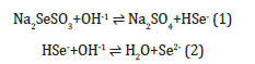
The deposition of GaSe thin films occurs when the ionic product of Ga2+ and Se2- ions exceeds the solubility product of GaSe. The control of Ga2+ and Se2- ions in the bath controls the rates of precipitation and the film formation and the equations of the deposition process is given [15] as follows: The hydrolysis of sodium Selenosulphate (Na2SeSO3) in the bath to give Se2- ions the following reactions:
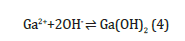
The reaction between Ga2+ and NaOH takes place through:

When the NaOH is added to the Ga2+ salt solution, the Ga(OH)2 begin to precipitate when the solubility product (SP) of Ga(OH)2 is exceeded, i.e
The GaOH precipitate dissolves in excess NaOH solution to form the complex sodium gallium hydroxide Na4Ga(OH)6 as follows:
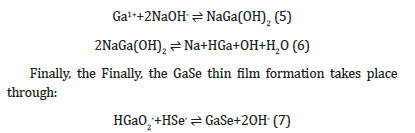
Figure 1 shows the optical absorption spectrum of electrodeposited gallium selenide film onto the ITO substrate in the visible region. The spectrum shows that the main absorption occurs in the wavelength region 350-450nm while additional absorption is also observed in the wavelength region of 450-550nm. This suggests that band-to-band optical transitions occur in the high photon energy region, while, on the other hand, transitions between the valence band and ionized donor or, alternatively, between an ionized acceptor and the conduction band appear in the lower energy region [15]. The absorbance data was further used to calculate the band gap energy of the gallium selenide film.
Figure 1:Plot absorbance against wavelength for gallium selenide thin film.

Figure 2:Current density Vs photon energy of GaSe thin films annealed.

Figure 3:Photoconductivity study of GaSe thin films.

Figure 2 shows the plots of current density Vs photon energy estimating the band gaps for both the as-deposited and the annealed thin films of GaSe at varied temperatures (i.e 200 °C, 300 °C, 400 °C, 500 °C and 600 °C). The energy band gaps estimated by extrapolating the straight-line portion of the plots for zero absorption coefficient values which gives an absorption energies corresponding to the band gap energies. The estimated band gaps are 2.89eV, 2.95eV, 3.08eV and 3.05eV for the as deposited thin film and the annealed thin films at temperatures of 200 °C, 300 °C and 500 °C respectively [21-25]. The band gap energy increases slightly as substrate temperature increases from 200 °C to 500 °C which indicates blue shifts from the normal bulk value and confirming that, annealing the films causes a red shifts of 0.19eV, 0.25eV, 0.38eV and 0.35eV in the optical spectra to that of characteristic bulk GaSe [15] and could be attributed to size quantization leading to quantum confinement of GaSe thin film [26]. Figure 3 shows the plots of currents (Dark and Photo) against the applied electric field which was used in analysing the photoconductivity of the GaSe thin film annealed at 300 °C. Both the photo and dark currents were observed to increase linearly with the applied electric field, but the former being large, and latter is less, which is an indication of positive photoconductivity which is caused by the generation of mobile charge carriers caused by absorption of photons. This is in agreement with the result of [27]. Since illumination produces electron-hole pairs and the holes neutralize the repulsive potential at the grain boundaries which leads to an exponential increase in the electron mobility that gives a high photo current under illumination, combined with the low dark current, it produces a high photosensitivity in the thin films [6].
Figure 4:ln σ versus T graphs of GaSe thin films.

The probability defect in the Group II samples is Se vacancies, as can be interpreted based on the activation energy from T versus ln σ graphs fits (Figure 4), since give the activation energy (~25meV) indicative of identical defects in both Se rich and Ga rich films. This observation that the material remains p-type with Se vacancies is in consonance with observation in Se deficient GaSe samples. The variation of photocurrent with applied voltage in CGSe films is shown in Figure 5. The photocurrent increases with an increase in voltage. Similar behavior of the photocurrent has been reported by Shahidi et al. [28]. Photocurrent spectra of GaSe films deposited at different duty cycles are shown in Figure 6. The photocurrent spectra show a peak near the absorption edge which was also observed by Rose [29]. The band gap of GaSe films determined from the spectral response is 1.68eV. This is in good agreement with the band gap value obtained from optical absorption measurements. The low photocurrent in the short wavelength range may be due to the high absorption coefficient and only surface region where defect states give a shorter lifetime, is excited. In the high wavelength region, the radiation is only partially absorbed giving rise to less photocurrent than the peak value. Tails of the spectra extending to 1200nm are attributed to direct excitation of the carriers from the defect levels. Similar results have been reported by several workers for GaSe films [30]. Figure 7 shows the variation of photocurrent with light intensity of GaSe films annealed at different temperature. The photocurrent is found to increase with an increase of temperature due to increase in light intensity. The J-V characteristics of the previous sample at light intensities 1100, 900, 700, 500 and 300w/ m2 have been shown. As can be seen, J-V characteristics of solar cells vary under different levels of illumination. Variation of the light intensity incident on a solar cell changes all solar cells parameters (Figure 8). The light generated current is proportional to the flux of photons therefore J is directly proportional to the light intensity [6- 7], While, open circuit voltage increases logarithmically with light intensity, as shown in the equation 8 below;
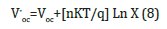
Where Voc is open circuit voltage at light intensity equal to 1100w/m2, X is the concentration of sunlight, for example, when solar cells illuminated under 700w/m2, X equal to 0.8 [31,32
Figure 5:Photocurrent-voltage characteristics of GaSe films annealed at different temperature..

Figure 6:Photocurrent-spectra of GaSe thin films annealed at different temperatures.

Figure 7:Photocurrent-illumination characteristics GaSe thin films annealed at different temperatures.

Figure 8:J-V curves for solar cells at different intensity.

Conclusion
GaSe has been used as a semiconductor, photoconductor, second harmonic generation crystal in nonlinear optics, GaSe also finds applications in high efficiency solar cells and battery technology. We found with excellent electrical properties and high sensitivity to visible light, gallium selenide exfoliated ultrathin films are particularly used in electronic and optical devices such as phototransistors, FETs, LEDs, and photovoltaics. GaSebased nonlinear optics have been advanced in many important applications such as integrated optics, optical information communications, biology, and imaging technologies. The sample slides were annealed in an oven at temperatures from 200 °C, into 600 °C and we studied optical and electrical properties. Annealing the films causes a redshifts of 0.19eV, 0.25eV, 0.38eV and 0.35eV in the optical spectra to that of the characteristic bulk GaSe and this was attributed to size quantization leading to quantum confinement of GaSe thin film and the photo and dark currents were observed to increase linearly with the applied electric field, but the former being large and latter is less, which is an indication of positive photoconductivity which is caused by the generation of mobile charge carriers caused by absorption of photons. Gallium Selenide crystals possess wide optical transparency, ranging from the wavelength of 0.65 to 18mm. One of the most important properties of bulk GaSe is its nonlinear optical property due to the absence of an inversion symmetric center.
References
- Kim S, Jahandar M, Jeong JH, Lim DC (2019) Recent progress in solar cell technology for low-light indoor applications. Current Alternative Energy 3(1): 3-17.
- Lim DC, Jeong JH, Pyo K, Lee D, Heo J, et al. (2018) Effect of emissive quantum cluster consisting of 22 Au atoms on the performance of semitransparent plastic solar cells under low intensity illumination. Nano Energy 48: 518-525.
- Kang R, Park S, Jung YK, Lim DC, Cha MJ, et al. (2018) High-efficiency polymer homo-tandem solar cells with carbon quantum-dot-doped tunnel junction intermediate layer. Adv Energy Mater 8(10): 1702165.
- Lohar GM, Thombare JV, Shinde SK, Chougale UM, Fulari VJ (2015) Preparation and characterization of iron doped zinc selenide thin film by electrodeposition. Journal of Shivaji University (Science and Technology) 41(2): 1-3.
- Seo KW, Lee SS, Park JP, Shim W (2006) Single-source precursor based ZnSe thin film preparation through MOCVD method. Bull Korean Chem Soc 27(12): 2074-2076.
- Oztas M, Bedir M, Bakkaloglu OF, Ormanci R (2005) Effect of Zn:Se ratio on the properties of sprayed ZnSe thin films. ACTA Physica Polonica A 107(3): 525-534.
- Sharma J, Shika D, Tripathi SK (2014) Optical and electrical properties of ZnSe thin films: Effect of vacuum annealing. Romanian Reports in Physics 66(4): 1002-1011.
- Godillo G, Calderon C, Rojas F (2003) Determination of optical constants of ZnxIn1-XSe thin films deposited by evaporation. Revista Mexicana De Fisica 49(4): 329-334.
- Desai HN, Dhimmar JM, Modi BP (2015) Study of linear and non- linear optical parameters of zinc Selenide thin film. Inter Jour Engr Res Appl 5(6): 117-122.
- Antohe S, Ion L, Mihaela G, Toma O (2013) Optical and morphological studies of thermally vacuum evaporated ZnSe thin films. Romanian Reports in Physics 65(3): 805-811.
- Pawan K, Aravind K, Parvinder, Kapi M (2012) Study of wavelength dependence of optical constants for ZnSe vacuum evaporated thin films. Inter J latest Res Sci Tech 1(4): 342-344.
- Lokhande CD, Patil PS, Tributsch H, Ennaoui A (1998) ZnSe thin films by chemical bath deposition method. Solar Energy Materials and Solar Cells 55(4): 379-393.
- Okereke NA, Ekpunobi AJ (2011) ZnSe buffer layer deposition for solar cell application. Journal of Non-Oxide Glasses 3(1): 31-36.
- Annuar K, Ho SM, Tan WT, Atan SK, Nagalingam S (2011) Chemical bath deposition of ZnSe thin films: SEM and XRD characterization. Euro Journ Appl Sci 3(3): 113-116.
- Ezema FI, Ekwealor ABC, Osuji RU (2006) Effect of thermal annealing on the band gap and optical properties of chemical bath deposited ZnSe thin films. Turk Journ Phys 30: 157-163.
- Pandurang CP, Santosh TM, Rangrao VS, Lalasaheb PD (2013) Structural, morphological and optical studies of ZnSe thin films: Growth using chemical bath. Advances in Applied Science Research 4(3): 177-181.
- Durdu BG, Alver U, Kucokunder A, Sogut O, Kavgaci M (2013) Investigation on zinc selenide and copper selenide thin films produced by chemical bath deposition. ACTA Physica Polonica A 124(1): 41-45.
- Xu TN, Wu HZ, Si JX, Cao CF (2007) Observation of triangle pits in PbSe grown by molecular beam epitaxy. Appl Surface Sci 253(12): 5457-5461.
- Pathan HM, Kale SS, Lokhande CD, Han SH, Joo OS (2007) Preparation and characterization of amorphous manganese sulphide thin films by SILAR method. Mater Res Bull 42(8): 1565-1569.
- Kassim A, Nagalingam S, Tee TW, Karrim MJ, Haron Ho SM (2009) Cyclic voltammetry synthesis of ZnS thin films using triethanolamine as a complexing agent. Analele Universitatii din Bucuresti-Cimie 8: 59-66.
- Pankove JI (1971) Optical processes in semiconductors. Dove Publications, New York, US, p. 91.
- Islam MR, Podder J (2009) Optical properties of ZnO nano fibre thin films grown by spray pyrolysis of zinc acetate precursor crystal. Research and Technology 44(3): 286-292.
- Janai MD, Alfred DO, Booth DC, Seraphim BO (1979) Optical properties structures of amorphous silicon films prepared by CVD. Sol Ener Mater 1(1-2): 11-27.
- Bube RH (1960) Photoconductivity of solids. In: Robert E (Ed.), Krieger Publishing Co. New York, US.
- Bruno U, Haowen X (2013) Theoretical analysis of the spectral photocurrent distribution of semiconductors. INTECH Open Science Ch 8: 191-206.
- Mohanty T, Pradhan A, Gupta S, Kanjilal D (2004) Nanoprecipitation in transport matrices using an energetic ion beam. Nanotechnology 14: 1620.
- Thirumavalavan S, Mani K, Sagadevan S (2015) Investigation on the photoconductivity of ZnSe, ZnS and PbS. Scientific Research Essays 10(10): 362-366.
- Shahidi AV, Shih I, Champness CH (1955) Photoconductivity and extrinsic doping of p-CuInSe2. Sol Energy Mater 12(5): 383-389.
- Rose A (1955) Space charge limited currents in solids. Phys Rev 97: 1538-1544.
- Kazmerski LL, Hallerdt M, Ireland PJ, Mickelsen RA, Chen WS (1983) Optical properties and grain boundary effects in CuInSe2. J Vac Sci Technol 1(2): 395-398.
- Kim WN, Park SW, Jeon CW (2014) Origin of performance loss in post-deposition Na-treated Cu(In,Ga)Se2 solar cell. Thin Solid Films 550: 587-590.
- Kronik L, Rau U, Guillemoles JF, Braunger D, Schock HW, et al. (2000) Interface redox engineering of Cu(In,Ga)Se2- based solar cells: oxygen, sodium, and chemical bath effects. Thin Solid Films 361-362: 353-359.
© 2023 A A Elamin. This is an open access article distributed under the terms of the Creative Commons Attribution License , which permits unrestricted use, distribution, and build upon your work non-commercially.
Editor In Chief


.jpg)


Signup for Newsletter

Quick Links
 Editorial Board Registrations
 Submit your Article
 Refer a Friend
 Advertise With Us
Our Recent Edition

.jpg)


Top Editors


.jpg)


.bmp)
.jpg)
.png)
.jpg)


.jpg)


.png)

.png)


.png)


Financial Support

Sponsors

Latest e-Books

Latest Video

 a Creative Commons Attribution 4.0 International License. Based on a work at www.crimsonpublishers.com.
Best viewed in
a Creative Commons Attribution 4.0 International License. Based on a work at www.crimsonpublishers.com.
Best viewed in