
- About Us
- Information
-

The Author ensures that the research has been conducted responsibly and ethically with adherence to all relevant regulations. read more..
- For Authors
- For Reviewer
- Manuscript Guidelines
- Membership
- Publication Ethics
-
- Journals
- Reprints
- e-Books
- Videos
- Policies
- Contact Us
 COVID-19
- Submissions


Full Text
Aspects in Mining & Mineral Science
Humidity Sensing of SnO/Porous Silicon Heterojunctions
Dzhafarov TD*, Bayramov AH, Ragimov SX, Imanaliyev AR, Bagiyev EA, Karimova AM, Asadullayeva SG and Jalilli JN
Institute of Physics, Azerbaijan National Academy of Sciences, Azerbaijan
*Corresponding author: Dzhafarov TD, Institute of Physics, Azerbaijan National Academy of Sciences, Azerbaijan
Submission: April 26, 2022;Published: May 04, 2022

ISSN 2578-0255Volume9 Issue2
Abstract
A nanoparticle metal oxide SnO thin film fabricated on Porous Silicon (PS) is studied as a subject for room temperature humidity sensing device application. The structural, photoluminescence, optical and electrical properties of thin films and SnO/PS/Si heterostructures are studied. Current-voltage characteristics of SnO/PS/Si heterojunctions are measured under normal atmosphere and humid environment in the range of 62-95% RH. The humidity-resistance effect, i.e., decrease of resistance between contacts to SnO and Si substrate under humidity exposition is obtained for SnO/PS/Si heterostructures at room temperature. The structure shows well pronounced response-recovery behavior (response time about 1min) after successive cycles of placing in humid environment. The similar dependence is observed for the capacitance under humidity. The mechanism for the humidity-stimulated electricity in SnO/PS/Si sensor at room temperature is discussed.
Keywords: Nanoparticle SnO; Porous silicon; SnO/PS/Si heterostructure; Humidity-stimulated of resistance
Introduction
Porous Silicon (PS) has attracted attention due to wide variety of possibilities for environmental monitoring, clinical diagnostics, homeland security, automotive, photo-electronics and other applications [1-3]. Interest of porous silicon materials is very intestive in the recent years due its potential applications and gas sensors, in various areas such as air-quality monitoring, fuel cells, biomedical sciences chemical industries etc. Effect of humidity on electrical properties, optical and photoluminescence spectra of free-standing porous silicon and PS samples have been studied [4,5]. The crystalline structure of porous silicon presents a network of silicon in nano (micro)-regions with an extremely large surface-to-volume ratio (up to 800m2/cm3). The structure of porous silicon is like a sponge or columnar where quantum confinement effect plays fundamental role. The pore surfaces are covered by silicon hydrides (Si-H) and silicon oxides (Si-O). Existence of pores, especially the canal-form pores, which determine ion (proton) conductivity along opens new perspectives for using porous silicon-structures as gas sensors. PS is characterized also by high chemical activity of the surface. These properties enable PS to effectively react with gases and PS layers are therefore considered as very promising for gas sensor applications. Gas sensors are divided to next main categories: resistive, capacitive, solid electrolyte, infrared and other. The resistive sensors are created on the basis of tin oxide (SnO2) or similar metal oxide semiconductors (CuO, ZnO, TiO2 etc.). The working principle of this type of sensor is that the resistance of metal oxide semiconductor changes when it is exposed to the ambient gas, i.e., gas reacts with the heated metal oxide surface and changes its electronic properties. One limitation of metal oxide gas sensors, however, is their operation temperature (350-500 °C) must be led to high power consumption. Humidity of porous silicon sensors principle, mechanism, fabrication technologies were examined in [6]. New type of sensors for humidity and hydrogen based on metal (Ag, Au, Cu)/PS Schotky structures has been proposed in [7-10]. Metal/PS Schotky-type structures operating as humidity-sensitive sensors or sensors sensitive to hydrogen- containing gases do not need to operate under an external voltage bias. Instead, such structures in humid or hydrogen-containing atmospheres produce electricity by themselves. In other words, metal/PS structures exhibit the properties of both a gas sensor and a hydrogen fuel cell.
The sensitivity behaviors of the Au/n-SnO2/p-PSi/c-Si sensors
to H2 and CO2 gases were achieved sensitivity, accordingly about
60% and 95% at temperature 250-300 °C [11]. Pt-catalysed SnO2/
Porous-silicon hybrid sensor of CO increased by a factor of 7.5
compared to the ones on for 10min and c-Si (at 100 °C) [12]. Influence
of the deposition temperature on Ammonia gas sensing of SnO2/
Porous silicon structure investigated and sensing characteristics
depicted at the room temperature and quick response and recovery
times at the deposition temperature of 350 °C [13]. SnO2-based
sensors has received attention in the field of toxic gas detection due
to their high sensitivity, fast response and long-term stability [14].
Synthesis of ZnO-SnO2 nano-thin films on porous silicon or glass
as NH3 gas sensing conducted in [15]. The prepared gas sensors
of mixed ZnO-Sn02 give a highest sensing response for 63ppm
NH3 on glass substrate at 200 °C. The sensitivity of the prepared
on the glass is better than on porous silicon. Significant sensing
response of SnO2/porous silicon heterojunctions could be obtained
at sufficiently high temperature [11-13]. The crystallin (for
example, lattice constants (a,c)), and band gaps of SnO and SnO2 are
significantly different [16].
To the best of our knowledge, the data on properties of the SnO/
Porous silicon-based sensors is lacking in literature. In this study,
the humidity sensing of SnO/PS/Si heterojunction has been studied
and the effectiveness of the SnO/PS/Si-based sensing device has
been shown.
Experimental Procedure
Monocrystalline p-type boron-doped silicon wafers with of orientation of (100), resistivity about of 10Ω cm and thickness of about 200μm were used for fabrication of SnO/PS/Si heterojunctions. The electrical contacts were made by screenprinted with a Du Ponta photovoltaic silver paste for front and silver with 3% aluminum paste for the back contact. Samples with silver contact baked at 200 °C for 10min. and metallization was carried out at 800 °C for 10min. in the conventional annealing furnace [9,10]. Porous silicon layers with of 10-20μm an average porosity of 47-80 % were prepared on p-type Si substrates by anodic etching in HF: H2O = 1:3 solution at a dc current of about 5mA/cm2 for 20min. The average porosity (P), i.e., the void fraction in the porous layer was evaluated by gravimetric method using the equation:
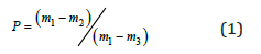
Here m1 is sample mass before the etching, m2 after etching and m3 after the removal of porous layer completely by rapid dissolution of the porous layer in 3% KOH solution. The thickness of porous silicon (d) was measured from:
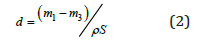
Where ρ is the silicon density (2.33g/cm3) and S is the etched
surface.
Thin film of the pure tin (Sn) of about 100nm was deposited
onto silicon, porous silicon and glass substrates by evaporation
in vacuum (5x10⁻⁵ bar). The thickness of the film was measured
using a deposition controller (Inficon, Leybold). Conversion of Sn
to n-type SnO was performed by oxidation in air at 300 °C for 10h.
The efficiency of the humidity response was defined as the ratio of
the resistance difference under air (Ra) and humidity (Rh) to that in
the air (Ra):
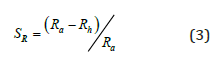
Current-voltage characteristics of n-SnO/p-PS/p-Si heterojunctions were measured in air and humid environment in special chamber. Resistances of SnO/p-PS/p-Si heterojunction were calculated from direct I-V-characteristics at fixed value of V=2V. The Relative Humidity (RH) was changed by evaporating of water inside of the chamber from 62% to 95% RH and measured by using “Extech-444701’’ Hydron Thermometer. The capacitance values were measured using the IET 1920 Precision LCR meter at 1MHz frequency. X-Ray Diffraction (XRD) analyses of the films were carried out using Bruker D2 Phaser (Germany) diffractometer in θ-2θ (10-70°) scan mode with Ni-filtered CuKα radiation (λ=1.54060 A) source. Photoluminescence (PL) measurements were performed using PL/PLE/Raman spectrometer (Tokyo Instruments, Inc.). The emission of the samples was excited by 325nm wavelength laser beams. The spectrometric ellipsometry measurements in 190– 1700nm spectral range were performed using Woollam M2000 rotating compensator instrument. Incident light angles were varied between 55° and 65° with 5° step. The Complete Ease computer program was used for the ellipsometric data fitting procedure. All of the measurements were performed at room temperature.
Results and Discussion
Figure 1: XRD patterns of the SnO film on glass substrate.

Typical XRD pattern of obtained SnO layer formed on glass
is shown in Figure 1. The XRD patterns reveal narrow peaks,
characteristic for tetragonal lattice with a=3.8020 A and c=4.8360 (Space group: P4/nmm) of the obtained films in agreement
with the JCPDS card N° 01085 0423. The average grain sizes of
SnO calculated using the Scherer formula from Full-Width Half-
Maximum (FWHM) were found to be 64nm. The dense of SnO film is
6.399g/cm3. The photoluminescence spectrum of SnO film on glass
substrate is displayed in Figure 2. The spectrum consists in a few
wide bands at 1.75eV, 2.3eV, 2.9eV and a shoulder at about 3.3eV.
The band around 3.3eV can be evidently attributed to intrinsic
optical transition in SnO film. This assumption is supported by
spectroscopic ellipsometry measurements shown in Figure 3. The
transition at about 3.3eV (see, imaginary part ɛ2 of the dielectric
function) is obviously due to the absorption at the fundamental
band gap of SnO, which is also in good agreement with the optical
absorption results, obtained in [17]. As for low-energetic bands in
the PL spectrum, they generally can be related to crystal defects or
defect levels associated with oxygen vacancies, or tin interstitials
that have formed during growth process [17]. Figure 4 illustrates the
humidity dependence of resistance for SnO/PS/Si heterostructures.
It is seen that resistance decreases from 55kΩ to 10kΩ with
increase of the relative humidity from 65 to 95% RH. The humidity
sensitivity of resistance of SnO/PS/Si heterostructure sensor at
room temperature is about of 80%. The essential dependence on
relative humidity shows also heterostructure capacitance which
increases from 650nF to 780nF (Figure 4). It should be noted
that for n-SnO/p-Si (without PS film) and p-PS/p-Si structures the
noticeably change in I-V characteristics under humidity was not
observed. Figure 5 shows the response-recovery behavior of direct
current at V=2V of the SnO/PS/Si sensor after successive cycles of
placing in a humid environment. It can be seen that the response
time is about 1min.
To summarize, the following experimental facts related to
change of the electrical characteristics after placing the SnO/PS/
Si heterostructures in humid atmosphere (300K) were solidly
established:
Figure 2: Photoluminescence spectrum of SnO film on glass substrate.

XRD analyses of the nanoparticle thin films SnO n-type (about 100nm) prepared by oxidation the pure tin to SnO film in air at 300 °C, show tetragonal lattice with a=3.8020 Å, b=4.8360 Å and the average grain sizes of SnO about 64nm.
Figure 3: Real (ɛ1) and imaginary (ɛ2) parts of dielectric function of SnO film on glass substrate.

Figure 4: The dependence of resistance and capacitance of SnO/PS/Si heterostructure on relative humidity.

Figure 5: The current response of SnO/PS/Si sensor as a function of storage time on the successive placing in air (65%RH) and humid environment (95%RH).

The photoluminescence and optical measurements show that
forbidden band around 3.3eV can be attributed to intrinsic optical
transition in SnO film.
Placing SnO/PS/Si structures in humid environment results in
both the forward and reverse current of I-V characteristics.
For SnO/PS/Si structures the forward conductivity increases
(resistance decreases from 60kΩ to 10kΩ) with rise of the relative
humidity (from 65 to 95% RH).
This phenomenon is reversible, for SnO/PS/Si structures,
inserting and removing the structure from H2O is the response and
recovery of the conductivity.
However, when the SnO/Si structures (without PS film) were
placed in a humid environment, noticeable electricity change was
not observed.
The gas-stimulated function mechanisms for resistance or
capacitance type porous silicon-based sensors are generally
associated with a change in the carrier concentration in porous
layer due to the absorbed molecules or change in dielectric constant
as a result of gas concentration inside the pores. In contrast to gasstimulated
mechanism, the mechanism involved in the sensing
response of SnO/PS/Si heterostructure to humidity is rather
complicated. The sensing mechanism consists in the dissociation
of H2O molecules at the surface of the SnO nanostructure [12]. One
of the two O-H bonds cleaves resulting in one OH- that bond to Sn4+
sites, meanwhile H+ bonds to an oxygen atom from the SnO lattice.
The H+ ions, which diffuse into n-SnO and meet with free electrons,
become neutral. Both hydrogen and OH- particles passing cross of
the n-SnO/p-PS contact reaches the nanostructure region of p-PS [8].
Further, the concertation of holes increases because of interaction
of H2 and OH- with nano-defects of the p-type porous silicon (Si-O
and Si-H grains). In fact, thickness of the hole accumulation layer
increases (the resistance decreases) in nanostructure porous
silicon and therefore the resistance decreases with increase of
humidity in SnO/PS/Si heterojunction.
Conclusion
SnO thin films are fabricated on porous silicon, silicon, glass substrates by means of conversion of pure Sn into SnO by oxidation in air at 300 °C for 10h. The structural, optical and electrical properties of thin films SnO and SnO/PS/Si heterostructures are studied. Thin films reveal a tetragonal symmetry (Space group: P4/nmm) with lattice parameters a=3.8020 Å and c=4.8360 Å and average grain size of 64nm. The current-voltage characteristics of SnO/PS/Si heterostructures are measured at humidity and at room conditions. Humidity-resistance and humidity-capacitance effect of SnO/PS/Si heterostructures are observed with the sensor response to H2O molecules about of 30% (at relative humidity 65-95%). The mechanism for humidity-stimulated electricity in SnO/PS/Si heterostructures is discussed.
References
- Dzhafarov TD, Bayramov AB (2017) Porous silicon and solar cells. handbook of porous silicon. In: Canham L (Edt.), Springer, Germany, p. 1479.
- Barillano G, Nannet A, Piere F (2003) ASFET: New, porous silicon-based gas sensing device. Sensors and Actuators B 93: 263-270.
- Ramirez GF, Garcia SG, Rosendo E, Diaz T, Caballero FN, et al. (2020) Porous silicon gas sensors: The role on the layer thickness and the silicon conductivity. Sensors 20: 4942.
- Dzhafarov TD, Aydin S, Oruc LC (2007) Effect of humidity on optical and electrical properties of free-standing porous silicon films. Transactions of National Academy of Science of Azerbaijan XIII(5): 17-20.
- Kayaham E (2015) Porous silicon-based humidity sensors. Acta Physica Polonica A 127(4): 1397-1399.
- Farahini H, Wagiran R, Hamidon MN (2014) Humidity sensors principle, mechanism and fabrication technologies: A comprehensive review. Sensors 14(5): 7881-7939.
- Dzhafarov TD, Can B (2000) Humidity-voltaic characteristics of Ag/PS/Si structures. J Mater Sci Lett 19: 2193.
- Dzhafarov TD, Oruc C, Aydin S (2004) Humidity-voltaic characteristics of Au-porous silicon interface. J Phys D: Appl Phys 37: 404.
- Dzhafarov TD, Aydin YS, Oruc LC (2008) Porous silicon-based gas sensors and miniature hydrogen cells. Japanese Journ of Appl Phys 47(10): 8204 -8207.
- Dzhafarov TD, Can OB, Oruc C, Allahverdiev ZA (2002) Hydrogen sensing characteristics of Cu-PS-Si structures. J Phys D: Appl Phys 35: 3122-3126.
- Muhsien MA, Salem ET, Agool IR, Hamdan HH (2014) Gas sensing of Au/n-SnO2/p-PSi/c-Si heterojunctions devices prepared by rapid thermal oxidation. Appl Nanosci 4: 719-732.
- Gonzales DMR, Kumar Y, Ramon JAR, Bogy RNKR, Mendez SFO, et al. (2022) CO2 sensing performance enhanced by Pt-catalysed SnO2/porous-silicon hybrid structures. Sensors International 3: 100165.
- Alwan AM, Abed HR, Yourif AA (2021) Effect of the deposition temperature on ammonia gas sensing based of SnO2/porous silicon. Plasmonics 16: 501-509.
- Li B, Zhou Q, Peng S, Liao Y (2020) Recent Advances SnO2–based sensors for detecting volatile organic compounds. Front Chem.
- Jasim MN, Al-Jumaili HS (2019) Synthesis of ZnO- SnO2 nano films on porous silicon as NH gas sensing performance. Journal of Engineering and Applied Sciences 14(5): 9056-9061.
- Kaizra S, Bellal B, Louafi Y, Trara M (2017) Improved activity of SnO for the photocatalytic oxygen evolution. J Saudi Chemical Society 22(1): 76-83.
- Cheng B, Russell J, Shi W, Zhang L, Samulski E (2004) Large-scale, solution-phase growth of single-crystalline SnO2 nanorods. J Am Chem Soc 126(19): 5972-5973.
© 2022 Dzhafarov TD. This is an open access article distributed under the terms of the Creative Commons Attribution License , which permits unrestricted use, distribution, and build upon your work non-commercially.
Editor In Chief


.jpg)


Signup for Newsletter

Quick Links
 Editorial Board Registrations
 Submit your Article
 Refer a Friend
 Advertise With Us
Our Recent Edition

.jpg)


Top Editors


.jpg)


.bmp)
.jpg)
.png)
.jpg)


.jpg)


.png)

.png)


.png)


Financial Support

Sponsors

Latest e-Books

Latest Video

 a Creative Commons Attribution 4.0 International License. Based on a work at www.crimsonpublishers.com.
Best viewed in
a Creative Commons Attribution 4.0 International License. Based on a work at www.crimsonpublishers.com.
Best viewed in