- Submissions

Full Text
Aspects in Mining & Mineral Science
Effect of Time and Angle Etching in the Performance Heterojunction Si Solar Cells
El Amin AA*
Department of Physics, Faculty of Science, Aswan University, Egypt
*Corresponding author: A A El Amin, Department of Physics, Faculty of Science, Aswan University, Aswan, Egypt
Submission: June 01, 2021;Published: September 01, 2021

ISSN 2578-0255Volume7 Issue3
Abstract
In this paper, Glancing Angle Deposition Technique (GLAD) has been used to grow Silicon (Si) thin film by vacuum thermal method on glass substrates. Heterojunction with Intrinsic Thin-Layer (HIT) solar cells are sensitive to interface state density. Traditional texture process for silicon solar cells is not suitable for HIT one. Thus, Sodium Hydroxide (NaOH), Isopropanol (IPA) and mixed additive were tentatively introduced for the texturization of HIT solar cells in this study. Then, a mixture including nitric acid (HNO3), Hydrofluoric Acid (HF). The morphology of textured surface and the influence of etching time on surface reflectance were studied, and the relationship between etching time and surface reflectance, vertex angle of pyramid structure was analyzed. It was found that the mixture consisting of 1.1 wt% NaOH, 3 vol% IPA and 0.3 vol% additives with etching time of 60min is the best for HIT solar cells under the condition of 80 °C. By used SEM and optical properties the average surface reflectance was 11.68%. Finally the effect of different processes on the performance of HIT solar cells was investigated. Films deposited at large angles (00, 100, 200, 300, 450, 600) was found to be poly-crystalline in nature along the peak intensity direction. The surface morphology has shown an improvement without the presence of secondary phases for higher incident angles (45°). It has been observed that the use of this growth technique leads to an improvement in the optical properties of the films.
Keywords: Si; Thin films; GLAD technique; Structural properties; Optical properties; Electrical characteristics
Introduction
Crystalline Silicon (C-Si) is the industrially dominant component in most solar cell manufacturing due to its non-toxicity at high level material control, natural abundance, high carrier mobility, and industry compatibility [1-3]. Similar to any photovoltaic technology, increasing the efficiency and reducing the cost are of prime interest. Reducing the cost involves using less material by developing thinner wafers and enhancing the efficiency and cost of the manufacturing processes. It also includes reducing the cost of the solar system including the antireflective layers and the tracking system. However, the PV industry based on C-Si is limited due to high cost fabrication for large scale applications and high reflection losses which limit their efficiency and their use [4-7]. Possible solutions are using AR coatings to suppress reflection and high aspect ratio nanostructures to increase absorption by increasing the optical path of photon [2,8,9]. However, most common AR coatings are limited in use due to their chemical, thermal and mechanical instability with the thin film and their validity only for certain wavelengths and certain incident angles [2,9]. The limitation of the traditional AR coatings for certain wavelength and angle range such as using SiNx layer as AR coating on silicon based solar cells reduced the reflection from 40% to 6% only with normal incidence, is very common problem [9]. Therefore, using AR coatings for wide wavelengths and angles range is inefficient, requires high cost for multilayer use and for a mechanical tracking system to follow the solar radiation at different angles [2,9]. In the last few years, Black Silicon (B-Si) paved the way not only for highly efficient Si solar cells but also for a wide range of applications ranging from energy applications like lithium ion batteries [10], hydrogen production through water splitting [11], sensing applications [12,13] and photonic devices [14-16]. B-Si is widely preferred for solar energy harvesting applications due to its unique morphology. This morphology changes the effective index at Si-air interface thereby reducing the reflection and leading to increased absorption and increased short circuit current density of solar cell [17]. The first solar cell based on black silicon had efficiency 1.6% [18]. The optical absorption and the minority carrier lifetime are very important parameters in determining the efficiency of solar cells [19]. More research and developments are still undertaken to offer better control on the solar cell parameters towards high efficiency till reach 22.1% [20]. Therefore, researchers are looking for methods to produce.
Experiments
The c-Si substrates (FZ, N-type, 1-10 Ω.cm) with (100) surface orientation were used. Before texturization, the c-Si substrate was cleaned with acetone and alcohol (analytical reagent) in ultrasonic cleaning equipment, in order to wipe off organic contaminations. For wafer saw damage etching, 10 wt% NaOH was used at 80 °C for 150s. For the pyramidal texturing, 1.1 wt% NaOH solution with 3 vol% IPA as a wetting agent and 0.3 vol% additives were used. Following etching in NaOH, the wafers went with an RCA2 clean, or both RCA2 clean and acid etching. The RCA2 solution consisted of 2:3:6 HCl : H2O2 : H 2O, heated to 80 °C for 10min. Si films of different thickness have been prepared from Si by evaporation in a vacuum-coating unit ((Edwards E306A) at room temperature. Si was placed in a molybdenum boat. Commercial glass substrates of thickness 8m were used to deposit Si films. A high vacuum of the order of 10-5 Torr was employed by a turbo-pump. Edward’s film thickness monitor FTM-7 was used to monitor the thickness of the films during evaporation. The distance between source and substrate was kept 7cm for all samples to obtain homogenous and uniform film thickness of large area. The surface morphology of the wafers was analyzed with a SUPERTM 55VP Scanning Electron Microscope (SEM). The reflectance of the textured silicon surfaces were measured from 400 to 1100nm by equipment with an integrating sphere. The current–voltage characteristics (I-V) of the HIT solar cells were measured under calibrated 100mW/cm2 AM 1.5G irradiance at room temperature (33 °C). growth of pyramids tended to be balanced. Pyramid size changed toward uniform. The standard deviation showed a low numerical value. When it came to 60min, the standard deviation was less than 0.1%. Pyramids distributed uniformly. Reflectance of textured samples was much lower than those polished and as-cut wafers for wavelengths between 400 and 1100nm.
Results and Discussion
As HIT solar cells are sensitive to interface state density, the best etching time of HIT solar cells was 60min using alkaline solutions to etch. SEM micrographs of HIT substrate sample with 60min etching time were shown in Figure 1. As it can be seen, pyramid structure completely covered the surface of silicon wafers and distributed uniformly. The gap between large pyramids and small pyramids is not big. The exceeding small pyramids on the boundary of large pyramids in traditional texture process can cause epitaxial grown [21] (Figure 2). In the short wavelength range before 500nm, the performance for each curve is similar. Samples at etching 60min represent better spectral responses compared with the other samples at the middle wavelength range from 500 to 900nm. This may be due to the relatively exceptional rear-side passivation provided by the si films on the flatter surfaces; photogenerated electrons at the bottom of wafer are therefore easily repelled to the p-n junction for collection. As for wavelengths over 900nm, an obvious difference in spectral response occurs as well. The smoothed surface of sample etching 60min that is functionally analogous to a mirror facilitates the reflection of more unabsorbed long-wavelength light back to the active region of the Si bulk. For convenience, the reading number at 950nm wavelength was used to indicate the reflectance of a measured point. To evaluate the uniformity of the reflectance, five spots were measured across the surface of each sample wafer and then an average value along with standard deviation was calculated, as show in Figure 3. With the increase of etching time, the standard deviation showed a trend of decrease after the increase. Reflectance R spectra of Si films, deposited at different incident angles without substrate rotation, are presented in (Figure 4) respectively. The spectra show interference patterns with a sharp fall of transmittance at the band edge, which is an indication of an acceptable crystallinity. It was also observed that the oscillations are not very damped as the obliquely angle deposition is increased, in particular for low incident angles which can be explained by the thickness variations. From the transmittance spectra, we note that the absorption edge was displaced to the low wavelengths as increases. Considering the conductive and anisotropic properties, the sheet resistances measured as a function of the evaporation angle of deposition plane are shown in (Figures 5 & 6). Due to the glancing angle deposition, the thin films are porous, so that the sheet resistance of GLAD Si thin films is larger than that of normal Si thin films. The sheet resistance increases with deposition angle due to the increasing porosity. Because of the anisotropic column structure, the sheet resistance parallel to the deposition plane is larger than that perpendicular to the deposition plane. As the flux incident angle becomes larger, more voids are introduced into the thin films.
Figure 1: SEM micrographs of silicon wafer with different etching time (30,45,60,90min).

Figure 2: IQE (Internal Quantum Efficiency) vs wavelength for silicon wafer with different etching time (30,45,60,90min).
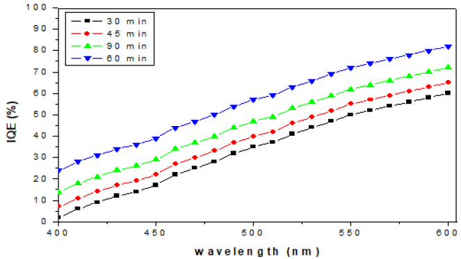
Figure 3: Effects of etching time on the uniformity of reflectance across a wafer.

Figure 4: Change of reflection with incident angle for Si substrate.
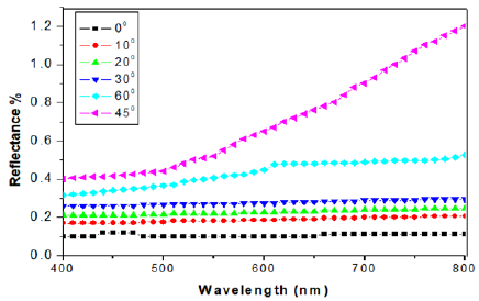
Figure 5: Absorption spectra of the Si thin films at different evaporation angles.
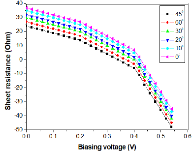
Figure 6: The sheet resistance vs. deposition angles for Si thin films.

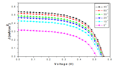
Moreover, the grain boundary potential also increases. The thin film resistance increases because the probability of an electron scattering at the grain boundary with higher potential increases [22]. The columnar distance of direction parallel to the deposition plane is larger than that of the direction perpendicular to the deposition plane. Hence, the sheet resistance parallel to the deposition plane is much larger. Where, different deposition conditions were introduced to prepare the thin film solar cells. A substrate temperatures (Ts) at RT of 300K and dopant weight percentage of (0.5, 1.5, and 2.5) of 5N purity of Al for n-type and Sb for p-type to form a p-n junction thin film solar cell( i.e., Si p-n junction). The cell performance of the GLAD Si films has shown large variations with the incident angle of deposition. In terms of short circuit current density, (Jsc) and the overall solar conversion efficiency of the cells. The open circuit voltage (Voc) is about 0.6V and the fill factor is 70.6%. All the films were deposited at a relatively low substrate temperature at 20 °C, resulting in films of comparable crystallinity and thus similar Voc. The Jsc is directly linked to the amount of light absorbed and converted by the cell, so it is influenced mainly by the value of evaporation angle of deposition. However, the amount of light trapped and the quality of Si photoanode that determines the electron diffusion efficiency can also affect Jsc. Photoanode of Si in the anatase phase of high crystallinity will improve the transport of injected electrons, reduce recombination with the electrolyte and result in higher quantum efficiencies. The GLAD films with connected open pores likely improve the accessibility of the entire film internal surface to the dye and to the electrolyte, leading to a more direct path for the injected electrons (Figure 7). Furthermore, the columnar nature of the GLAD films provides a more direct and shorter path for electron transfer. The results of their simulation and actual preparation of GLAD Si films indicated that the effective surface area is enhanced by oblique deposition owing to columnar formation and becomes maxima at a deposition angle of 60°. The films deposited at 60° possess the maximum effective surface area and the best photovoltaic performance. The fill factors of the Si films are 71-77%, much higher than most of the reported values in literature [23,24]. As the fill factor is influenced by the interfaces of the major components in Si. The overall efficiencies of the GLAD Si thin film in this study were decided largely by their Jsc. As such, the cells with Si layer annealed at higher temperatures to enhance crystallinity and with thicker Si layer to increase the amount of dye absorption will likely increase Jsc values and the overall efficiency.
Figure 7: Shows the photovoltaic measurements of n-Si/p-Si glass substrate thin films.
Conclusion
As HIT solar cells are sensitive to interface state density, the best etching time of HIT solar cells was 60min using alkaline solutions to etch. In the short wavelength range before 500nm, the performance for each curve is similar. Samples at etching 60min represent better spectral responses compared with the other samples at the middle wavelength range from 500 to 900nm. Five spots were measured across the surface of each sample wafer and then an average value along with standard deviation was calculated. The spectra show interference patterns with a sharp fall of transmittance at the band edge, which is an indication of an acceptable crystallinity. Due to the glancing angle deposition, the thin films are porous, so that the sheet resistance of GLAD Si thin films is larger than that of normal Si thin films. A substrate temperatures (Ts) at RT of 300K and dopant weight percentage of (0.5, 1.5, and 2.5) of 5N purity of Al for n-type and Sb for p-type to form a p-n junction thin film solar cell( i.e., Si p-n junction). The fill factors of the Si films are 71-77%, much higher than most of the reported values in literature [23,24]. As the fill factor is influenced by the interfaces of the major components in Si. The overall efficiencies of the GLAD Si thin film in this study were decided largely by their Jsc.
References
- Mrazkova Z, Sobkowicz IP, Foldyna M, Postava K, Florea I, et al. (2018) Optical properties and performance of pyramidal texture silicon heterojunction solar cells: Key role of vertex angles. Photovolt Res Appl 26(6): 369-376.
- Lin G, Gao Z, Gao T, Chen Y, Geng Q, et al. (2020) Research progress in improving the performance of PEDOT:PSS/Micro-and Nano-textured Si heterojunction for hybrid solar cells. Journal of Materiomics 7(5): 1161-1179.
- Lu YT, Barron AR (2013) Nanopore-type black silicon anti-reflection layers fabricated by a one-step silver-assisted chemical etching. Phys Chem Chem Phys 15: 9862-9870.
- Srivastava SK, Kumar D, Schmitt S, Sood K, Christiansen S, et al. (2014) Large area fabrication of vertical silicon nanowire arrays by silver-assisted single-step chemical etching and their formation kinetics. Nanotechnology 25(17): 175601.
- Han N, Wang F, Ho JC (2012) One-dimensional nanostructured materials for solar energy harvesting. Nanomaterials and Energy 1: 4-17.
- Razek SA, Swillam MA, Allam NK (2014) Vertically aligned crystalline silicon nanowires with controlled diameters for energy conversion applications: Experimental and theoretical insights. J Appl Phys 115(19): 194305.
- Chen LJ (2007) Silicon nanowires: the key building block for future electronic devices. J Mater Chem 17: 4639-4643.
- Oh J, Yuan HC, Branz HM (2012) An 18.2%-efficient black-silicon solar cell achieved through control of carrier recombination in nanostructures. Nat Nanotechnol 7(11): 743-748.
- Cai J, Qi L (2015) Recent advances in antireflective surfaces based on nanostructure arrays. Mater Horiz 2: 37-53.
- Chan CK, Peng H, Liu G, McIlwrath K, Zhang XF, et al. (2008) High-performance lithium battery anodes using silicon nanowires. Nat Nanotechnol 3(1): 31-35.
- Oh J, Deutsch TG, Yuan HC, Branz HM (2011) Nanoporous black silicon photocathode for H2 production by photoelectrochemical water splitting. Energy Environ Sci 4(5): 1690-1694.
- Gamal R, Ismail Y, Swillam MA (2015) Optical biosensor based on a silicon nanowire ridge waveguide for lab on chip applications. J Opt 17(4): 045802.
- Miu M, Kleps I, Pavesi L, Craciunoiu F, Ignat T, et al. (2007) Nanostructured silicon for optical biosensors. In Semiconductor Conference, IEEE, pp. 345-348.
- Qian F, Gradecak S, Li Y, Wen CY, Lieber CM (2005) Core/multishell nanowire heterostructures as multicolor, high-efficiency light-emitting diodes. Nano Lett 5(11): 2287-2291.
- Thonissen M, Berger MG, Kruger M, Billat S, Fischer RA, et al. (1996) Optical interference filters made of porous silicon. MRS Online Proceedings Library Archive, vol. 431.
- Steglich M, Zilk M, Bingel A, Patzig C, Kasebier T, et al. (2013) A normal-incidence PtSi photoemissive detector with black silicon light-trapping. J Appl Phys 114(18): 183102-183108.
- Kumar D, Srivastava SK, Singh PK, Sood KN, Singh VN, et al. (2010) Room temperature growth of wafer-scale silicon nanowire arrays and their Raman characteristics. J Nanopart Res 12(6): 2267-2276.
- Sarnet T, Carey JE, Mazur E (2012) From black silicon to photovoltaic cells, using short pulse lasers, in AIP. Conference Proceedings, Phipps, 1464: 219-228.
- Otto M, Algasinger M, Branz H, Gesemann B, Gimpel T, et al. (2015) Black silicon photovoltaics. Adv Opt Mater 3(2): 147-164.
- Savin H, Repo P, Gastrow GV, Ortega P, Calle E, et al. (2015) Black silicon solar cells with interdigitated back-contacts achieve 22.1% efficiency. Nat Nanotechnol 10: 624-628.
- Gouda AM, Allamc NK, Swillam MA (2017) Efficient fabrication methodology of wide angle black silicon for energy harvesting applications. RSC Advances 7(43).
- Hochbaum AI, Gargas D, Hwang YJ, Yang P (2009) Single crystalline mesoporous silicon nanowires. Nano Lett 9(10): 3550-3554.
- To WK, Fu J, Yang X, Roy V, Huang Z (2012) Porosification-reduced optical trapping of silicon nanostructures. Nanoscale 4: 5835-5839.
- Ebbesen TW, Lezec HJ, Ghaemi H, Thio T, Wolff P (1998) Extraordinary optical transmission through sub-wavelength hole arrays. Nature 391: 667-669.
© 2021 El Amin AA. This is an open access article distributed under the terms of the Creative Commons Attribution License , which permits unrestricted use, distribution, and build upon your work non-commercially.
 a Creative Commons Attribution 4.0 International License. Based on a work at www.crimsonpublishers.com.
Best viewed in


.jpg)


 Editorial Board Registrations
 Submit your Article
 Refer a Friend
 Advertise With Us

.jpg)


.jpg)


.bmp)
.jpg)
.png)
.jpg)


.jpg)


.png)

.png)


.png)


