- Submissions

Full Text
Aspects in Mining & Mineral Science
Self-Assembling Photonic Crystals?
Samo Kralj1* and Mitja Kralj2
1Faculty of Natural Sciences and Mathematics, University of Maribor, Slovenia
2ŠKUC, Slovenia
*Corresponding author: Samo Kralj, Faculty of Natural Sciences and Mathematics, University of Maribor, Slovenia
Submission: September 01, 2020;Published: October 07, 2020

ISSN 2578-0255Volume5 Issue4
Opinion
Figure 1: The central atom (e.g., carbon or silicon) of valence four is linked with four neighboring atoms, which could result in a tetrahedral crystal structure.
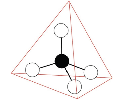
Various materials have dominated different human history periods. Some of them are even named by them: the Stone Age, Bronze Age, Iron Age… For example, in 5000 BC chisels made of copper (bronze is an alloy consisting primarily of copper) enabled the construction of Egyptian pyramids and sparked the growth of 1st great civilizations. From this perspective, the last century could be referred to as the Silicon Age. The “king” of this period, the silicon atom, is dressed with the electron cloud described by 1s2 2s2 2p6 3s2 3p2. Among these electrons, the outer four valence electrons, located at the 3s and 3p-orbital, are the most important for its “social” activities. These valence electrons can form a tetrahedral lattice crystal unit (Figure 1) characterized by a specific electronic band gap structure, displaying semiconducting electric behavior. This property is extremely useful, and due to its electronic semiconductors are at the heart of classical computers. The microelectronic revolution of the 20th century is based on sensitive control of electric currents in semiconductors, enabled by their band gap structure. The switching of logic functions relies on the number of electrons and holes below and above the band gap separating the valence and conducting band. Here the electronic band gap corresponds to a forbidden zone of energies that electrons cannot occupy. Among various semiconducting material, doped silicon is most commonly used. In addition to the band gap property, its main advantages with respect to competing materials were its natural abundance, optical transparency, and widespread use. In the 1980s first artificial photonic crystals appeared [1,2]. Crystal structures enabling sensitive manipulation of light beams have been demonstrated. Prototype photonic materials displayed periodic structures on a micrometer scale and possessed a photonic band gap. The latter is characterized by a window of optical wavelengths that cannot propagate through the otherwise optically transparent material. For example, the 1st photonic crystal was made by drilling a closely spaced array of sub micrometer sized cylindrical holes. These holes play a similar role as atoms in semiconductors. The band gap structure depends on the crystal symmetry and geometric parameters determining the crystal lattice. The parameters are tailored to yield the band gap in the visible wavelength regime. Again, as in the case of electric semiconductors, the tetrahedral geometry enabled desired properties, suggesting that this structure is outstanding for making a photonic band gap material. The general aim is to reproduce in photonic crystals analogous phenomena seen in electronic semiconductors. They should function as “semiconductors for light”. The key to this in the band gap structure, which is dictated by geometry. Note that the behavior of i) electrons and ii) light beams in i) electronic semiconductors and ii) photonic materials is governed by different basic equations: i) Schrodinger equation and ii) Maxwell equations, respectively.
Figure 2: a) A representative topological defect within an ordering field. In bulk, the ordering field tends to be spatially homogeneous, oriented along a single direction. The defect is characterized by the winding number m=1. At the defect origin, the ordering field is not uniquely defined. The defect core corresponds to the region where the elastic distortions due to the defect presence are relatively strong. In LCs the linear size of the core equals few nm. b) If an object is inserted within the defect core (in the figure the object is spherical), which weakly interacts with the ordering field, it reduces local energy costs introduced by the defect. c) In general, curvature enforces topological defects within the surface hosting the field. In the figure, there are two topological defects, characterized by m=1, located at the poles of the sphere. In the case of a vector field, such defects represent “elementary defects” (i.e., |𝑚|=1 corresponds to the minimal possible winding number). If the field exhibits head-to-tail invariance, “elementary defects” carry |𝑚|=1/2. Consequently, such geometry would in most cases host four m=1/2 TDs. d) In general, curved regions attract TDs. In the case shown, a m=1 defect covers the top of a cylindrically symmetric object. This placement of the defect enables the parallel structure of the ordering field below the defect, which is energetically advantageous.
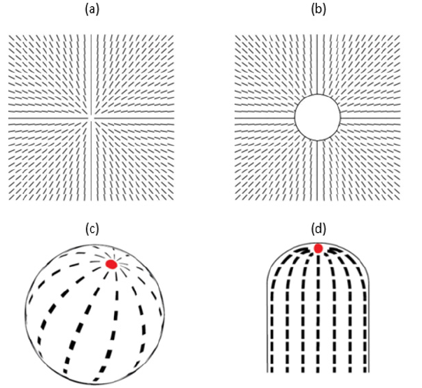
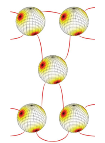
Already now photonic materials pervade our day-to-day life. They are present in several displays, smartphones, medical devices… Furthermore, they are promising to pave the way to completely new artificial materials, metamaterials, which are currently not present in nature. These materials are expected to introduce qualitatively new behaviors and functionalities. However, current photonic materials are made using “top-down” approaches, for instance, by etching, material deposition, 3D printing or drilling. It would be advantageous to produce such materials by exploiting some kind of “bottom-up” technology by exploiting materials possessing self-assembling property. One branch of such materials represent colloidal crystals [3] consisting of colloidal objects (particles) dispersed in an isotropic liquid. The surface of a particle should exhibit some (mesoscopic) in-plane ordering field, which in the case of non-toroidal geometry [3] unavoidably hosts topological defects (TDs) [4-6]. These TDs refer to points where the ordering field is not uniquely defined, as shown in Figure 2. Furthermore, the so-called binders (one-dimensional flexible nanoparticles, for example, polymer segments) should be homogeneously dispersed in the liquid matrix [3]. These binders should exhibit a strong tendency to attach to TDs and consequently bind together nearby particles. The resulting system is expected to exhibit crystal-like long-range structure (Figure 3), analogous to “nature-formed” crystals consisting of nm-sized atoms. In this analogy, particles play the role of atoms. The valence of these atoms is determined by TDs [3,6], and could be manipulated. Namely, the mechanisms i) determining the number and position of TDs, and ii) their binder-attraction tendency, are determined by relatively simple and robust mechanism. For example, one could exploit i) geometry [7-10], and ii) general tendency that appropriate nanoparticles are attracted to defects [11,12], respectively. The 1st mechanism is well embodied in the Effective Topological Charge Cancellation (ETCC) mechanism [8,9] and Curvature potentials [10]. They determine how a local curvature attracts or repels TDs [8-10,13,14]. Curvature enforced existence and attraction of appropriate TDs is illustrated in (Figure 2), respectively. The origin of the 2nd (the so-called Defect Core Replacement (DCR) [11,12]) mechanism, reflects the fact that the penalty of introducing otherwise energetically costly defects into an ordering field could be reduced if the defect core hosts an appropriate nanoparticle (Figure 2). Namely, in this case, a relatively energetically costly defect core is replaced by a volume of a nanoparticle trapped within it. Such systems could be formed by nematic shells [3,6,9,15,16] dispersed in an isotropic medium containing an appropriate concentration of nano-binders. A nematic shell consists of a colloidal particle covered by a thin nematic liquid crystal (NLC) layer, where the layer thickness is comparable to the characteristic LC molecular length. Typical NLCs [7,17] consist of rod-like molecules exhibiting head- to-tail symmetry (i.e., they have the symmetry of a cylindrical object). The corresponding nematic molecular field determines the local orientation of NLC molecules at the mesoscopic level. The molecular field tends to be spatially homogeneously aligned along a common symmetry breaking direction in bulk samples. However, owing to curved particle surface topological defects inevitably arise due to topological reasons [4,5] if a colloid does not possess toroidal topology [8] (i.e., it does not possess one hole). A possible structure is shown in Figure 2, where the NLC structure exhibits two defects characterized by the winding number (also termed the two-dimensional topological charge) m=1. The winding number [7] of a defect is determined by the number of total rotations of the nematic molecular field along any path encircling the center of defect counterclockwise. The winding number is a discrete and conserved quantity and its sign could be either positive or negative. Due to the head-of-tail symmetry, the minimal value of |𝑚| equals ½. It bears several similarities with electrical charges. Therefore, TDs bearing the same charge mutually repel and TDs bearing opposite charges attract and could eventually annihilate into a defect less state. Note that the total winding number mt within a nematic layer is determined by the topology. For example, for the spherical topology, it holds mt=2 [3,6], as shown in Figure 3. Therefore, for a perfect sphere, one expects four “repelling” m=1/2 TDs which tend to maximize their mutual separations [6]. Hence, such an atom exhibits valence equal to four like silicon, its “real-atom” analog. Note that one could control position and even number of TDs by varying colloidal curvature. Shapes of nematic shells could be flexible. For example, biological membranes exhibiting some kind of in-plane order [10] are effectively similar to nematic shells. One could relatively easily change their shape by, for example, changing their relative volume v [11] (The latter is defined as the ratio between the volume of a membrane with its volume if it is spherical, while the total membrane surface is fixed) [18].
Figure 3: A self-assembling unit consisting of atoms (e.g., nematic shells) exhibiting valence four, which is determined by the number of TDs. In the case shown each nematic shell possesses four m=1/2 defects. The regions possessing relatively high local energy penalties due to the presence of defects are indicated with the red color. The centers of defect cores of nearby atoms are linked by binders (for instance, flexible polymers which are indicated by red colored lines).
To conclude, there is a strong interest to develop self-assembling colloidal crystals with a controllable valence of constituting atoms. By remotely controlling the valence of atoms (e.g., by an external electric field, temperature, pressure…) one could form a rich variety of crystals exhibiting different symmetries. Note that symmetry plays a key role in determining physical macroscopic properties. Further, the valence (i.e. the number of TDs and their position) could be in general strongly manipulated in atoms, yielding even configurations, which are not present is classical crystals. Resulted materials could be exploited as efficient light controlling element with numerous potential engineering and biomedical applications.
References
- Lindley D (2013) Landmarks-The birth of photonic crystals. Physics 6: 94.
- Yablonovitch E (1987) Inhibited spontaneous emission in solid-state physics and electronics. Phys Rev Lett 58(20): 2059-2062.
- Nelson DR (2002) Toward a tetravalent chemistry of colloids. Nano Lett 2(10): 1125-1129.
- Poincaré H (1886) Dissertation on the curves defined by a differential equation. J Math Pure Appl 2: 151.
- Kamien RD (2002) The topological theory of defects in ordered media. Rev Mod Phys 74: 953.
- Vitelli V, Nelson DR (2006) Nematic textures in spherical shells. Phys Rev E 74(2): 021711.
- Lavrentovich OD (1998) Topological defects in dispersed liquid crystals, or words and words around liquid crystal drops. Liq Cryst 24(1): 117-125.
- Bowick M, Nelson DR, Travesset A (2004) Curvature-induced defects unbinding in toroidal geometries. Phys Rev E 69(4): 041102.
- Mesarec L, Góźdź W, Iglič A, Kralj S (2016) Effective topological charge cancelation mechanism. Sci Rep 6: 27117.
- Mesarec L, Góźdź W, Iglič A, Iglič VK, Virga EG, et al. (2019) Normal red blood cells' shape stabilized by membrane's in-plane ordering. Sci Rep 9(1): 19742.
- Kikuchi H, Yokota M, Hisakado Y, Yang H, Kajiyama T (2002) Polymer-stabilized liquid-crystals blue phases. Nat Mater 1(1): 64-68.
- Karatairi E, Rozic B, Kutnjak Z, Tzitzios V, Nounesis G, et al. (2010) Nanoparticle-induced widening of the temperature range of liquid-crystalline blue phases. Phys Rev E 81(4): 041703.
- Selinger RLB, Konya A, Travesset A, Selinger JV (2011) Monte Carlo studies of the XY model on two-dimensional curved surfaces. J Phys Chem B 115(48): 13989-13993.
- Napoli G, Vergori L (2012) Extrinsic curvature effects on nematic shells. Phys Rev Lett 108(20): 207803.
- Skačej G, Zannoni C (2008) Controlling surface defect valence in colloids. Phys Rev Lett 100(19): 197802.
- Kralj S, Rosso R, Virga E (2011) Curvature control of valence on nematic shells. Soft Matter 7: 670-683.
- Muhoray PP (2007) The diverse world of liquid crystals. Phys Today 60: 54.
- Guo DY, Chen CW, Li CC, Jau HC, Lin KH, et al. (2020) Reconfiguration of three-dimensional liquid-crystalline photonic crystals by electrostriction. Nat Mater 19: 94-101.
© 2020 Samo Kralj. This is an open access article distributed under the terms of the Creative Commons Attribution License , which permits unrestricted use, distribution, and build upon your work non-commercially.
 a Creative Commons Attribution 4.0 International License. Based on a work at www.crimsonpublishers.com.
Best viewed in


.jpg)




 Editorial Board Registrations
 Submit your Article
 Refer a Friend
 Advertise With Us
.jpg)



.jpg)


.bmp)
.jpg)
.png)
.jpg)


.jpg)




.png)

.png)


.png)
