- Submissions

Full Text
Annals of Chemical Science Research
Variation of Band Gap in Graphene Grown by Plasma Enhanced Chemical Vapor Deposition
Chang-Soo Park1 and Heetae Kim2*
1Department of Physics, Sejong University, Seoul 05006, Korea
2Rare Isotope Science Project, Institute for Basic Science, Daejeon 34047, Korea
*Corresponding author: Kim H, Rare Isotope Science Project, Institute for Basic Science, Daejeon 34047, Korea
Submission: March 11, 2020Published: March 16, 2020

Volume2 Issue1January, 2020
Abstract
We report the transport behavior of graphene grown by plasma enhanced chemical vapor deposition (PECVD). The graphene films were grown at 950 °C for 5, 10, 30 and 60min, respectively. Raman spectra showed that the synthesized films are bilayer with strong defect peaks. The temperature dependent conductivity of graphene films showed the band gap modulation with increasing growth times. Thermally activated (TA) conduction model showed that the values of band gap of graphene films are 95, 73, 48 and 36meV for 5, 10, 30 and 60min growth times, respectively.
Keywords: Graphene; Raman; Band gap; PECVD; Defect
Introduction
Graphene is a two-dimensional monolayer with linear dispersion relation near the Dirac point and has attracted much interest owing to its superb material properties, such as very high mobility of 10,000 cm2/Vs at room temperature and quantum hall effect to promise for the potential in nanoelectronics [1-4]. However, graphene is a semimetal without an energy band gap which is required to be used as an electronic transistor. Recent studies have shown that band gap is formed at various situation, in nanoribbons, [5] bias-applied, and [6] strained or molecule-doped graphene [7,8]. Though the band gaps were generated in various structures, the control of the electrical properties is still a challenge. On the other hand, defects and impurities in graphene are important in electrical transport, because scattering is a hurdle in carrier transport in graphene, making the modulation of graphene transport quite important for physical and device application. In particular, defects in graphene have been intensely studied because quasi-localized states near the Fermi energy can be induced due to vacancy [9,10]. Here, we report that band gap engineering has been achieved by PECVD growth and plasma treatment can induce modulation of the defective properties of graphene. The graphene films were synthesized by plasma-enhanced chemical vapor deposition (PECVD) at 950 °C on sapphire substrate without catalyst, and the radio frequency plasma power was fixed at 150W. Carrier gas was argon (300sccm) and hydrogen (30sccm). The hydrocarbon, CH4 (1sccm) was used as a source precursor during the growth. Growth time was adjusted from 5min to 60min. Pristine graphene was identified as a bilayer using an optical microscope and Raman signal. Raman spectra of the graphene films were measured at an excitation of 514.5nm at room temperature using a spectrometer (Horiba Jobin-Yvon, HR800UV). The electrical transport was characterized as a function of temperature using low temperature measurement system (Sungwoo Instrument & Sumitomo).
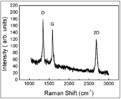
Figure 1 shows the Raman spectra of graphene film grown on sapphire substrate for 5min by PECVD. The D band (defect) intensity of the graphene grown by PECVD is relatively very high compared with that of usual graphene grown by thermal CVD methods. The defect peaks were strong at 1350cm-1 due to plasma effect and the ratio of I2D/IG is approximately close to unity as shown in Figure 1, indicating that this sample is, in fact, the bilayer graphene [11].
Figure 1: Raman spectra of graphene synthesized by PECVD for 5min.

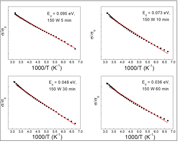
Figure 2 shows the temperature dependent conductivity of graphene synthesized by PECVD for 5(a), 10(b), 30(c) and 60min(d), respectively. The conductivity increased with increasing temperature, like a usual semiconductor, for the graphene films grown at 950 °C. According to the previous work, the temperature-dependent conductivity of graphene can be well explained by the thermally activated (TA) conduction equation. The TA model can be described as: σ=σ0exp(-Eg/2kBT), where Eg is the band gap energy, kB is the Boltzmann constant, and T is the absolute temperature in Kelvin, for high temperature regions over 100K, whereas variable range hopping mechanism is effective at low temperature [12]. The bandgap energy of 0.095eV was observed as shown in Figure 2 for the graphene synthesized for 5min, and then the value of band gap decreased gradually. It is well known that plasma irradiation generates many vacancies during the formation of graphene film [13]. Such vacancies in the graphene film synthesized by using PECVD result in defects. The origin of band gap formation is resulted from defects in the graphene [14]. Also, previous theoretical report predicted that the defects could induce a band gap in graphene. The formation of the band gap is owing to the breaking of sublattice and molecular symmetry in the graphene [15]. In this study, the vacancies in graphene could be generated during the growth by plasma radiation. The values of band gap of films are 95, 73, 48 and 36meV for 5, 10, 30 and 60min growth times, respectively. This means that the defects of graphene grown by PECVD were decreased as the growth time increases and the sample quality was improved by long time growth.
Figure 2: Temperature dependent conductivity of graphene synthesized by PECVD for 5(a), 10(b), 30(c) and 60(d) min, respectively. Red line means the fitting by conductivity equation.

Conclusion
In conclusion, we have studied the transport behaviors of graphene grown by PECVD. Band gap engineering was achieved in the temperature dependence of conductivity. TA conduction mechanism of transport was described for the band gap evaluation. TA conduction model showed that the values of band gap of films are 95, 73, 48 and 36meV for 5, 10, 30 and 60min growth times, respectively. Therefore, the band gap energy of graphene can be modulated by growth times, which enables graphene to have promising properties for electrical applications.
Acknowledgment
This work was supported by the National Research Foundation of Korea (NRF) grant funded by the Korea government (NRF- 2016R1D1A1B03932295).
References
- Novoselov KS, Geim AK, Morozov SV, Jiang D, Zhang Y, et al. (2004) Electric field effect in atomically thin carbon films. Science 306(5696): 666-669.
- Novoselov KS, Geim AK, Morozov SV, Jiang D, Katsnelson MI, et al. (2005) Two-dimensional gas of massless dirac fermions in graphene. Nature 438(7065): 197-200.
- Zhang Y, Tan YW, Stormer HL, Kim P (2005) Experimental observation of the quantum hall effect and berry's phase in graphene. Nature 438(7065): 201-204.
- Novoselov KS, Jiang Z, Zhang Y, Morozov SV, Stormer HL, et al. (2007) Room-temperature quantum hall effect in graphene. Science 315(5817):1379.
- Han MY, Zyilmaz OB, Zhang Y, Kim P (2007) Energy band-gap engineering of graphene nanoribbons. Phys Rev Lett 98(20): 206805.
- Zhang Y, Tang TT, Girit C, Hao Z, Martin MC, et al. (2009) Direct observation of a widely tunable bandgap in bilayer graphene. Nature 459(7248): 820-823.
- Guinea F, Katsnelson MI, Geim AK (2010) Energy gaps and a zero-field quantum hall effect in graphene by strain engineering. Nat Phys 6: 30-33.
- Ohta T, Bostwick A, Seyller T, Horn K, Rotenberg E (2006) Controlling the electronic structure of bilayer graphene. Science 313(5789): 951-954.
- Pereira VM, Guinea F, Lopes Dos Santos JMB, Peres NMR, Castro Neto AH (2006) Disorder induced localized states in graphene. Phys Rev Lett 96: 036801.
- Pereira VM, Lopes Dos Santos JMB, Castro Neto AH (2008) Modeling disorder in graphene. Phys Rev B 77: 115109.
- Ferrari AC, Meyer JC, Scardaci V, Casiraghi C, Lazzeri M, et al. (2006) Raman spectrum of graphene and graphene layers. Phys Rev Lett 97(18): 187401.
- Miyazaki H, Tsukagoshi K, Kanda A, Otani M, Okada S (2010) Influence of disorder on conductance in bilayer graphene under perpendicular electric field. Nano Lett 10(10): 3888-3892.
- Wang JJ, Zhu MY, Outlaw RA, Zhao X, Manos DM, et al. (2004) Synthesis of carbon nanosheets by inductively coupled radio-frequency plasma enhanced chemical vapor deposition. Carbon 42(14): 2867-2872.
- Oostinga JB, Heersche HB, Liu X, Morpurgo AF, Vandersypen LM (2008) Gate-induced insulating state in bilayer graphene devices. Nat Mater 7(2): 151-157.
- Peng XY, Ahuja R (2008) Symmetry breaking induced bandgap in epitaxial graphene layers on SiC. Nano Lett 8(12): 4464-4468.
© 2020 Prasad DSN. This is an open access article distributed under the terms of the Creative Commons Attribution License , which permits unrestricted use, distribution, and build upon your work non-commercially.
 a Creative Commons Attribution 4.0 International License. Based on a work at www.crimsonpublishers.com.
Best viewed in


.jpg)


 Editorial Board Registrations
 Submit your Article
 Refer a Friend
 Advertise With Us
.jpg)


.jpg)


.bmp)
.jpg)
.png)
.jpg)


.jpg)


.png)

.png)


.png)


